AMD's Zen 6 processors are out! Well, the EPYC 9006 family of server CPUs is out, anyway. These aren't chips that mere mortals like you and I can reasonably acquire, so there aren't really many third-party benchmarks out there yet, but somebody ran GeekBench 7 on one, and you know what that means: time for some wild speculation, such as the supposed 15% single-threaded IPC increase you might have seen reported this week. However, it isn't quite that clear yet. Well-known enthusiast and occasional leaker HXL (@9550pro) spotted the EPYC 9996 result, and now Russian enthusiast "three twenty six" (@326powah) has done a direct comparison with his Ryzen 7 9700X at the same clock.
Let's lay out the details: the AMD EPYC 9996 is an absolutely gargantuan server processor with 256 "Zen 6c" cores spread across eight "Monarch" CCDs with 32 cores apiece. Each CCD has 128MB of L3 cache, which is reportedly split into two 64MB domains for each 16-core CCX. This gives us 4 megabytes of L3 cache per CPU core, which happens to be the exact ratio that AMD has maintained since Zen 2. Meanwhile, 326's Ryzen 7 9700X is a desktop CPU with eight Zen 5 CPU cores and 32MB of L3 cache, giving it the same cache-per-core ratio yet an overall smaller local cache for the CPU cores, to say nothing of the 1GB of L3 cache on the full EPYC 9996.
Yes, 1GB of L3 cache. That enormous CPU is also served by a 1024-bit memory bus, likely running at 12,800 MT/s, giving it a colossal 1.64 TB/second of memory bandwidth. However, the specific benchmarks we're comparing here are single-threaded benchmarks, and as a result, they aren't likely to be bottlenecked by memory bandwidth on either machine; even 326's relatively pedestrian DDR5 memory at 6000 MT/s CL34 is more than sufficient for a single-threaded, lightly vectorized workload like Geekbench 7. Matching the CPU core clock rates at 4.1 GHz actually gives us a pretty decent core-to-core comparison of performance, even if all factors are not equal.
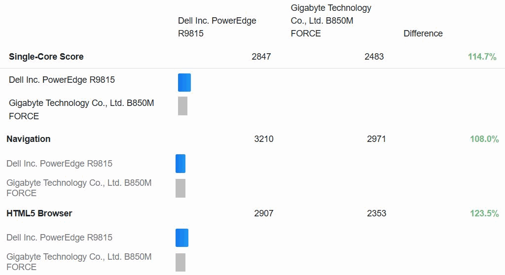
Comparing the Linux results, the gain over the desktop chip varies quite a bit depending on the specific test, but there are no regressions. (Image credit: @326powah on X)
So how does it come out? Frankly, it's a massacre. That's true whether we look at the Windows 11 results he posted first or the CachyOS Linux results that he posted later, although the Zen 5 part doesn't get embarrassed quite as badly in Linux. The Dell PowerEdge R9815 server hosting the big EPYC part scored 2847 in the single-threaded test; 326's Ryzen desktop scores 2483 in Linux and 2318 in Windows.
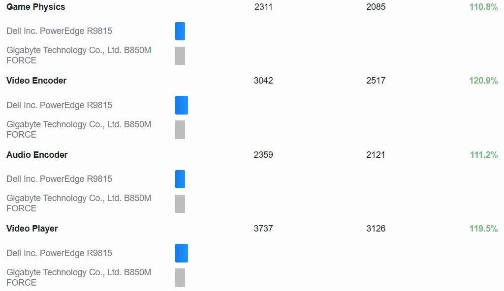
Looking at the Gala-to-Honeycrisp Linux results, the biggest performance gulf is some 24% in the HTML5 Browser test, which is normally quite sensitive to memory latency. That could easily be caused by the massive L3 cache of the EPYC CPU. Other tests aren't so easily dismissed by configuration mismatches, though. The 19% gain in asset compression, the 21% gain in video encoding, and the 17% gain in photo editing all point to real architectural differences between Zen 5 and Zen 6 that seem quite promising for its desktop debut next year.
What's fascinating is that these results won't have been affected much by the considerable SIMD horsepower of the Zen 6 CPU core, as Geekbench—at least historically speaking—makes relatively light use of CPU SIMD, and in fact, this specific test is marked as "AVX2," meaning it definitely isn't using the muscular AVX-512 units present in either CPU. In fact, most of these tests are actually measuring CPU integer arithmetic and memory subsystem performance more than raw CPU number-crunching power, so Zen 6 coming out so far ahead here is really interesting.
Media processing seems to be especially strong on Zen 6. (Image credit: @326powah on X)
Obviously, you shouldn't take this as gospel that "Zen 6 has 15% higher IPC than Zen 5," though that's arguably a plausible conclusion; there are just too many confounding factors to say that so far. Indeed, another one of those factors is that this isn't the Zen 6 CPU core that we'll be getting in desktop CPUs. The EPYC 9996 is a high-density part that uses Zen 6c, the specialized dense core design meant for increased area efficiency at the cost of its ability to scale to high clocks. After all, 4.1 GHz isn't exactly a high clock rate these days, and particularly not for chips manufactured on a bleeding-edge 2nm-class manufacturing process.
That's the part that should get you excited. Zen 5 had a very modest IPC uplift over Zen 4 (including even some regressions), and combined with a similarly modest clock rate gain, it wasn't a very exciting release for most desktop users. Zen 6 seemingly may have a significant IPC advantage as well as, if rumors hold, a fairly extreme clock jump over the current-generation parts. If that holds, this may be another leap like from Core 2 to Core i7, and these parts are confirmed to be coming to an AM5 socket near you. We'll be waiting with bated breath for the launch early next year. Hopefully there's RAM to buy by that point.
Having jettisoned 4F2 memory cells from its roadmap, Micron must use different methods to continue scaling its DRAM devices in the coming years to keep up with rivals planning to use smaller DRAM transistors towards the end of the decade. Instead, Micron intends to introduce wafer bonding with its upcoming 1ε DRAM process technology and adopt High-NA EUV lithography for subsequent generations. Meanwhile, the company is developing new types of memory, including vertical high-bandwidth memory (vHBM) and vertical edge inference memory (vEIM), which will be integrated directly on top of processors.
"DRAM is nearing atomic limits at this point," said Scott DeBoer, president and chief technology and products officer at Micron, during the company's event this week. "Although we have confidence in several more planar nodes, we are very focused on making sure that we introduce 3D DRAM at the optimal time from a cost and performance point of view."
Wafer bonding, High-NA EUV, and new materials
Micron's current 1γ DRAM process is already in high-volume manufacturing, whereas its successor, 1δ, is scheduled to enter volume production in the second half of 2027. The latter promises a mid-20% increase in bit density and is optimized for future AI memory products, including HBM5, vHBM, and vEIM. Beyond 1δ, Micron plans to introduce wafer bonding with its 1ε process, which is currently under development. However, the company has not disclosed how it intends to implement wafer bonding or what improvements it expects from the technology.
(Image credit: Micron)
For subsequent generations — ζÅ and ηÅ — Micron plans to adopt High-NA EUV lithography (ζÅ, zeta angstrom, Micron's 1st Generation sub-10nm-class DRAM node) and new materials (ηÅ, eta angstrom, Micron's 2nd Generation sub-10nm-class DRAM node) to continue shrinking DRAM cells. For many of its upcoming fabrication technologies that will be used over the next five to 10 years, Micron is also collaborating with Albany NanoTech. Of course, as with all organizations like Albany NanoTech, we are mostly talking about fundamental, or pre-competitive, IP that could be used for DRAM production at some point.
"Albany NanoTech, our announced focus on advanced lithography [is] really driving High-NA EUV roadmap for DRAM," said DeBoer. "In particular at Albany with our team there, focused on the next five to ten years."
(Image credit: Micron)
Micron is also developing 3D DRAM technologies and lists two generations — 3D1 and 3D2 — in its roadmap already. However, the company has not disclosed its architectures or launch schedules, as it intends to introduce 3D DRAM only when the technology offers sufficient advantages in manufacturing costs, complexity, and performance over conventional planar DRAM.
"When we look at three 3D DRAM we have that on the roadmap, as I mentioned, and it is shown here in between one zeta and one eta," said Micron's CTO. "But in reality, this is a parallel path, and we will implement it [3D DRAM] in a fashion that is ideal for cost, complexity, and device performance."
Going vertical, becoming critical
Beyond developing new process technologies for its upcoming DRAM products, Micron is also working on all-new types of DRAM products that are tailored for very specific use cases, including vertical HBM (vHBM), vertical edge inference memory (vEIM), and various custom HBM (cHBM) implementations.
(Image credit: Micron)
vHBM will place memory stacks directly on top of processors (such as AI accelerators and AI GPUs) rather than next to them. This approach promises substantially lower latencies and higher bandwidth thanks to shorter connections. However, placing memory above a processor creates significant thermal challenges and limits the number of memory stacks that can be integrated on top of an ASIC. Therefore, Micron expects vHBM to complement conventional HBM, which will continue to provide the bulk of memory capacity in many AI accelerators.
(Image credit: Micron)
Another technology under development is vertical edge inference memory (vEIM), which shares architectural and packaging characteristics with vHBM but targets different applications. Whereas vHBM prioritizes maximum bandwidth for high-performance AI accelerators, vEIM is focused on energy efficiency for edge AI processors used in autonomous vehicles, robotics, and other power-constrained devices. Nonetheless, even the 1st Generation vEIM targets formidable 2 TB/s bandwidth at <1pJ/bit energy, which is in line with what HBM4 currently offers (at 8 GT/s over a 2,048-bit interface). Micron intends to optimize these products with customers according to their bandwidth, capacity, and power requirements.
(Image credit: Micron)
Both vertical memory architectures will require advanced packaging technologies, particularly hybrid bonding, which enables much denser connections than conventional microbumps. Thermal management will also be critical, especially for vHBM. To meet cooling requirements, Micron is developing specialized heat-spreading structures to transfer heat from hot regions of memory base dies through the DRAM stacks.
The company has not disclosed when vHBM, vEIM, or cHBM will enter commercial production. What is important about the development of such types of memory is that it indicates that future improvements in memory performance will increasingly depend on advanced packaging and closer integration with processors, which will require collaboration between DRAM makers and logic developers. In turn, this transforms memory from a commodity to a critically important ingredient of an ASIC design.
Professional Windows crusher NTDEV has showcased their next-generation tool for compressing Windows 11 into the tiniest of tiny installs. Based on their newest and unreleased Pico11, they managed to create a “proof of concept I put together to see how small I could make a Windows 11 ISO while keeping a working desktop and a few familiar apps.” Moreover, it’s a perfect installer to shove on a 700MB CD-ROM without wasting space, with this demo version weighing in at 699,811,840 bytes.
The test system (a VM with 4GB allocated) used around 883MB of RAM.
In the above video, NTDEV demos a freshly installed Windows 11 ISO that had been processed with Pico11. The desktop looks familiar to anyone currently using Windows 11. “Calculator and Settings still open, Notepad saves files, and Paint still lets me draw questionable logos,” highlights the dev. However, it is also pointed out that “Task Manager might look a little older than you remember.” The older Task Manager seems to be a lightweight legacy version. It may have been possibly swiped from Windows 7, but its exact origin isn’t divulged by NTDEV.
At this time, NTDEV admits what you see is “an experiment, not a replacement for a normal Windows installation,” and that’s mainly because Windows Update and general servicing have been removed to fit inside the constraints of CDR capacity. If you are interested in creating Windows installs like this, the good news is that NTDEV says they are working on adding what they describe as Pico11 capabilities to the Tiny11 builder tool, which you can find on GitHub.
Tiny11 has already demonstrated impressive Windows 11 ISO building capabilities with its Tiny11 mode, Tiny11 Core mode, and Custom mode. Pico11 sounds most closely related to Tiny11 Core as it eschews servicing and recovery support. However, there appears to be some more under-the-hood tweaking, which may have been evidenced in this new showcase by the presence of the older version of Task Manager.
Tiny11 has historically been responsible for even smaller Windows 11 installs, but the extreme 100MB distillation of the OS, for example, came without any Windows 11 UI. Builds could also be remarkable for using tiny amounts of RAM – as little as 176MB. More typical and useful were custom builds powered by Tiny11 where 'bloatware' was removed and that weighed in at around the 2GB mark.
Hopefully we will learn more about Pico11 and get greater insight into its capabilities soon.
Cadence, one of the largest electronic design automation (EDA) companies, has unveiled Maestro, its new portfolio of domain-specialized AI models tailored for its chip design agents, in a press release sent just ahead of earnings. In initial results compared with general-purpose AI models, Cadence claims up to a 30% improvement in the quality of results and that Maestro effectively uses fewer tokens for the same task, with up to 5x the token efficiency. The first models “are available to select early access customers” in Q4 2026, and customers may run them on Cadence’s cloud, public clouds, or customer-controlled on-premises environments and post-train them on their own “proprietary data, designs, and workflows.” To learn more about Maestro, we spoke with two Cadence executives: Rob Knoth, senior group director of strategy and new ventures, and Paul Cunningham, senior vice president and general manager.
This approach is distinct from Synopsys’ own specialized model, GPT-Synopsys, which will run on OpenAI-hosted infrastructure, without using customer data to train the model. The models of both EDA giants, announced less than a month apart, now split on where a customer’s design data goes. Where they might not differ is why: Paul Cunningham, senior vice president and general manager at Cadence, told Tom’s Hardware Premium that agent costs have “really started to explode,” adding, “And I think the world realized so.” That makes it a natural step, he said, to move more of the agents’ iterating “into the weights of the models themselves.”
(Image credit: Cadence)
Maestro takes this step through Cadence’s AI Super Agents, which “interpret design intent, decompose tasks” and “orchestrate the Maestro portfolio with other leading frontier and open-weight models,” evaluating trade-offs to guide decisions with domain expertise. It also uses reinforcement learning (RL), where Cadence’s “deterministic solvers evaluate outputs against engineering objectives, constraints and ground truth,” and, importantly, the results feed back into the models for improvement.
The models include Nvidia’s Nemotron, and customers can run the customer-data training step themselves with Cadence’s fine-tuning harness, potentially “on their own GPUs, on their own network,” Cunningham said. He added that Nemotron, specifically, was “giving really solid results and actually improving very, very fast.”
One constant that keeps popping up with agentic EDA is the need to nail down what the numbers actually measure. In chip design, quality of results usually refers to the design’s power, performance, and area, though Cadence didn’t specify what its 30% figure measures. Both it and the 5x token efficiency figure are measured against “a general-purpose foundation model,” which Cadence told us is the open-source model Maestro started from before its training. The company wouldn’t name the foundational AI model that Maestro is derived from beyond mentioning that it is “one of the leading open source models that’s very competitive with commercial frontier models.”
Cadence credits the token savings to balancing its EDA and system design automation (SDA) “tool calls with LLM invocations.” As an analogy, Cunningham said, “You don’t need to drive to Safeway in the jet engine,” and you want to use “the right model at the right time for the right task.”
Runtime does matter, too: as Rob Knoth, senior group director of strategy and new ventures at Cadence, told Tom’s Hardware Premium in September that a tool call could take anywhere from hours to days to return a value, while the AI industry’s training loops are “used to minutes.” Efficiency could also lower costs, since Maestro use counts toward Cadence’s agent pricing, a subscription with a consumption allowance and charges for use beyond it, Cunningham said. He didn’t say whether the token savings cut a customer’s bill.
Being flexible for the customer is a key element of any solution, and for Cadence’s competitor Synopsys, this lies in Autopilot, which Synopsys says allows customers to “choose among commercial, open-source, and fine-tuned language models” across “Synopsys-managed and customer-managed deployments,” with cloud or on-premises infrastructure. For agent security, such as sandboxing, Cadence says it’s working with Nvidia on an integration with Nvidia’s OpenShell Reference Architecture, which Nvidia launched last week, naming both Cadence and Synopsys. These options can help protect customer intellectual property.
Cadence Maestro vs. GPT-Synopsys
Cadence Maestro
GPT-Synopsys
Announced
Oct. 26, 2026
Sept. 30, 2026
What it is
A portfolio of domain-specialized AI models for Cadence’s AI Super Agents
A specialized model that operates Synopsys’ tools directly
Model partner
Nvidia (Nemotron, OpenShell)
OpenAI
Models
Post-trained LLMs, trained decision models and agent skills, blended with frontier and open-weight models, including Nemotron
OpenAI frontier models
Where it runs
Cadence’s cloud, public clouds or customer-controlled on-premises environments
OpenAI-hosted infrastructure
Customer data
Customers can post-train it on their own data, designs and workflows, with Cadence’s fine-tuning tools
Customer data isn’t used to train the model
Claimed results
Up to 30% higher quality of results and up to 5x token efficiency vs. a general-purpose foundation model, the unnamed open-source model Maestro started from (initial results; measure not stated)
None disclosed
Availability
First models to select early-access customers in Q4 2026
No date; early technology engagements underway
Customers named
Socionext, Silicon Labs (Nvidia as partner)
None
Pricing
Subscription with a usage allowance, then charged by use
Not disclosed; Synopsys and OpenAI share revenue under their deal
Cadence has had a busy 12 months with customers and agents alike. During Cadence’s July earnings call, CEO Anirudh Devgan said ChipStack, its design and verification agent, “has more than 20 customer engagements,” and ViraStack, its custom and analog agent, “more than 25 customer engagements.” Socionext said just last week that it was applying InnoStack. Silicon Labs has also credited ChipStack with accelerating debugging, and both companies say they are watching Maestro next.
Cadence's agentic consolidation began with its acquisition of ChipStack back in November 2025. In June 2026, the company claimed that its agent had reached Level 5 autonomy, which we explored in detail. In September, Knoth teased Maestro’s ingredients to Tom's Hardware Premium a month early, two days before the GPT-Synopsys announcement: “reinforcement learning loops, domain-specific post-training of open-weight models, model routing.” Maestro is now sitting under all four super agents, targeting a similar year-end window to Synopsys’ Autopilot; the table below has the full timeline.
Done; co-founder Kartik Hegde now leads Cadence’s core AI research group
February 2026
ChipStack AI Super Agent
Up to 10x productivity for coding designs and testbenches, test plans, regressions and debug
In early access since launch
April 2026
ViraStack (custom and analog), InnoStack (digital implementation) and AgentStack (head agent)
—
Socionext is deploying InnoStack in production; others not stated
June 2026
ChipStack at Level 5, with Nvidia’s Nemotron and OpenShell
Over 40x faster RTL validation cycles in Nvidia’s deployment
Level 5 and AgentStack due to early-access customers in the second half of 2026
July 2026
AuraStack (PCB and advanced packaging)
Up to 2x faster time to market and 15x higher productivity
Available on Cadence’s Millennium M2000 supercomputer; Nokia is deploying it (Oct. 21)
September 2026
ChipStack RTL Generation Agent
An average of 24% less area and 18% less power than pure foundation-model code, in early evaluations
Due to select early-access customers in Q4 2026; early collaboration with Honda R&D
Oct. 26, 2026
Maestro AI Model Portfolio
Up to 30% higher quality of results and up to 5x token efficiency vs. a general-purpose foundation model, in initial results
First models available to select early-access customers in Q4 2026; about a dozen engagements
This rapid pace of progress means that a clear distinction has to be made between early access and general availability. Both Cadence and Synopsys can point to customer engagements, and, at least in the latter’s case for the AgentEngineer portfolio and Autopilot platform, general availability remains a goal by year’s end; Cadence hasn’t given a general availability date for Maestro. For GPT-Synopsys, though, only “early technology engagements are underway,” according to its partners. The platforms and agents remain works in progress.
For Maestro, Cunningham hopes for “more case studies, more quantifiable benefits” through Q4. The real story, as he aptly put it, is that “we’re going to bring agents and agentic AI natively into our vertical, not that our vertical is going to get embedded into general-purpose agents.” Only customer results on real workflows will test Cadence’s 30% number, but going by what both companies have shown so far, their own early figures are extremely promising and exciting for the EDA industry.
China is spending more time loitering near undersea cables in the Pacific Ocean than any other nation, according to a report by the Center for Strategic and International Studies, a U.S.-based think tank in Washington, DC. The analysis compared the behavior of 200 research vessels from 47 different nations, including the U.S. and Russia, and found that Chinese vessels spent a "statistically significant larger share of time" near critical infrastructure.
The analysis, reported by Indo-Pacific Defense Forum, notes that Chinese activity was particularly suspicious in this regard. It notes that the "persistent and disproportionate activity" means that China "may be leveraging its research fleet for underwater data collection that may aid... analysis of terrain for sabotage or submarine operations."
Civilian research vessels provide a unique cover for states looking for "plausible deniability" for their research gathering activities. The report mentions the activity of a ship from the Xiang Yang Hong research fleet which, between July and October 2024, spent time near three undersea cables that connected the U.S. with Australia, Indonesia, Singapore, Guam and others.
The ships move in a "lawnmower" pattern which, it notes, is associated with surveying to create accurate seafloor maps. While the ships themselves aren't part of the PRC's navy, the data they collect could be used to serve China in future conflicts.
These "gray zone research activities" continue in an era of Chinese conflict with its neighbors as it asserts territorial claims in the South China Sea against states like the Philippines and Vietnam, not to mention its claims over Taiwan, which Beijing considers a breakaway province.
Intel and AMD have spent decades competing for the processors inside PCs and data centers, but the rivalry hasn't stopped the two companies from working together when their interests align. And now, Intel CEO Lip-Bu Tan has reportedly discussed potential areas of cooperation with AMD chief Lisa Su, adding another possible partnership to the mix as Intel tries to regain its footing in the semiconductor industry.
According to a recording (embedded below) of Tan’s October 24 fireside chat with Chinese American Semiconductor Professional Association (CASPA) President Jimmy Cheng, the Intel CEO outlined his plans to rebuild the company’s CPU business, develop chips tailored to specific customer workloads, and attract more customers to its foundry operations. However, Tan did not publicly detail the reported areas of potential cooperation with AMD CEO Lisa Su.
Intel has traditionally built its business around its own processor roadmaps, but Tan says the company needs to be more flexible as customers look for silicon designed for particular workloads. He pointed to Intel's Xeon processors as one area where that approach is changing, alongside continued development of GPUs and accelerators.
"We have to reclaim the leadership in CPU. That is something that I am very determined to do." Tan said.
He also described a change in how Intel approaches customization. "Intel is so proud they never want to modify for customer needs," he said. "I'm modifying it for customer needs, and so that, I think, to me, is a fast-growing area, and I'm double, triple down on it."
The strategy extends beyond conventional CPUs, with Tan identifying application-specific integrated circuits (ASICs), co-packaged optics (CPO), physical AI, and advanced packaging as potential growth businesses. He wants two or three of these areas to eventually contribute around 10% of Intel's revenue each.
Intel's foundry business is another major part of Tan's plans. He said the company's 18A manufacturing process had reached volume production, while development of its next-generation 14A process was progressing strongly. Intel has already released version 0.5 of the 14A process design kit (PDK), which provides chip designers with the technical information and tools needed to develop products for the process.
Tan said version 0.9 was coming next, followed by version 1.0 for volume production in early 2027. "We have multiple customers [who] really want us to really scale their business," he said, referring to interest in Intel's foundry services.
However, Intel did not identify those customers or disclose the size of any potential manufacturing orders during the discussion. Notably, in January,Intel had two prospective customers evaluating 14A test chips, with firm supplier decisions expected during the second half of 2026 and the first half of 2027. Tan also described foundry manufacturing as a business where trust matters as much as technology. Customers hand over wafers that will eventually become products on which their own revenue depends, making missed deadlines or manufacturing problems costly. "The moment we take on the foundry, take on the wafer is a lot of responsibility to make them successful," he said.
He recalled one customer who had waited six to eight months hoping he would become CEO before presenting 15 areas where Intel had fallen short. Tan said he addressed the problems individually, after which the customer agreed to deepen its relationship with Intel.
That said, the prospect of further cooperation would not be entirely new. In October 2024, Intel and AMD established the x86 Ecosystem Advisory Group alongside other technology companies to coordinate improvements to the x86 instruction set architecture and make it easier for hardware and software developers to support both companies' processors.
That cooperation has since moved into AI software. Last week, it emerged thatAMD was integrating its ZenDNN optimizations into Intel's open-source oneDNN library, bringing the companies' CPU optimization work for PyTorch AI inference under a common software path. The companies have also worked together on Advanced Matrix Extensions and other x86 capabilities through the advisory group, showing that they cooperate on shared technologies while continuing to compete for customers. For now, however, neither company has announced a new agreement arising from the discussions.
AI has forced PC component prices up with no slowdown in sight over the last year. While building your own might be expensive, pre-built gaming PCs continue to offer the best value in many cases. With that in mind, you could secure a huge $1,070 discount on an Alienware Aurora gaming PC at Newegg right now, featuring an Nvidia GeForce RTX 5070 and 32GB DDR5 RAM for $2,199.99.
Dell's premium Alienware gaming brand usually comes with a price premium compared to budget or no-brand models. With this $1,070 discount applied, you're getting a rig for 4K-capable gaming at a fairer price than you would get by buying from Dell directly. Alongside the RTX 5070, this ACT1250 model ships with an Intel Core Ultra 7 265KF processor and a 1TB SSD.
Aurora ACT1250: was $3269.99 now $2199.99 This Alienware Aurora gaming PC is a powerhouse for 4K gaming. It features an Nvidia GeForce RTX 5070 GPU, a 20-core Intel Core Ultra 9 265KF CPU, 32GB of DDR5 RAM, and a 1TB SSD.View Deal
The GPU is often the big-selling feature in a gaming PC. With the Nvidia GeForce RTX 5070, you're getting one of Nvidia's latest Blackwell GPUs with 6,144 CUDA cores and 12GB of GDDR7 VRAM, operating on a 192-bit memory bus. What that means for gaming is that you've got a card that will smash through high frame rates, even with the highest graphics presets, at 1080p.
At 1440p, you're also going to see good performance, although the most demanding games might need a drop down or two. You can also fall back to using Nvidia DLSS with multi-frame generation for an uplift, powered by AI to add extra frames into the mix for smoother gameplay, especially if you want to game at 4K. Our GPU benchmarks show that the RTX 5070 is a strong option compared to its rivals, offering slightly better performance than the RTX 4070 it replaces.
You're getting an Intel Core Ultra 7 265KF CPU with this build. This is a 20-core Arrow Lake CPU with 20 cores, with eight good-for-gaming performance cores, along with 12 efficient cores for multi-threaded work. This is locked, meaning you can overclock it, and it ships with a max boost clock speed of 5.5 GHz.
This isn't a CPU able to compete with top-spec AMD rivals, but it's a solid enough performer when you couple it with the RTX 5070's power. Elsewhere, though, you're getting 32GB of DDR5 memory, so no compromises there. There's also a 1TB SSD, leaving you enough storage for at least a few big AAA installs.
The AI-powered inrush of software vulnerability reports over the last year has shined a light on how many critical pieces of open-source software are chronically underfunded. The latest victim is PHP, the scripting language powering about 71% of websites, making the news due to a critical remote code execution vulnerability. The PHP Foundation, which develops and oversees the language, reportedly counts only one full-time person and 14 "mostly part-time" contractors. That's bad enough, but the real problem goes far deeper thanks to the internet's lazy development practices and systems administration.
In an interview with Reuters, the PHP Foundation's Executive Director Elizabeth Barron spells it out clearly: she's the only full-time person on staff, and works with the contractors' help. Pertaining to the software itself, the team's job is to develop and maintain the PHP core, including taking care of security fixes. The core team accepts contributions from the world at large, in an arrangement not too dissimilar to Linux kernel development — except that project is far better-manned, with many full-time contributors and company-employed developers.
Naturally, the PHP foundation collaborates with other companies and many cybersecurity firms, but the dev team was stretched thin even before the increase in security vulnerabilities with the help of countless AI agents. Barron does note that there was no reported exploitation of PHP2Shell before the security fix came out.
But the lack of a higher funding level likely led to the "structural failure" to address the underlying vulnerability in a timely manner, as the out-of-memory condition (OOM) that eventually led to the 2026 exploits was originally discovered in 2024. Given how widespread PHP is, and how many third-party extensions there are, the work on fixing the OOM problem "stalled and restarted repeatedly over months." It didn't help that the Chainguard security firm broke the PHP2Shell embargo too early by accident.
Even still, the team is thankful for the money it has, as "without the Foundation’s funding it would have been impossible to have multiple people work on this issue full time, eventually through weekends and around the clock to coordinate and communicate with other involved parties." One would hope that this latest incident releases the purse strings of more companies that make their living off of PHP.
And yet, this failing is far larger than just bugs in the core language, which, notably, were only one point update away. In theory, any server running the current 8.x brand of the software should be upgraded in minutes with the released patches, but reality was far different, as websites went down for hours or days out of fear of exploitation.
The real problem reared its ugly head: nearly 73% of PHP installations were running versions well past their end-of-life (EOL) date, meaning that obtaining fixes is now far harder. Many professionals who worked with the language, including yours truly, had spent decades warning of this reckoning, even considering many Linux distributions were backporting fixes.
Many of these servers were still running PHP 7, a version that was completely EOL'd four years ago, with many years of advance warning, and that originally came out in late 2015, almost eleven years back. If that doesn't sound silly enough, let it sink in that around 7.7% of PHP sites were still running version 5.x, which first saw the light of day 22 years ago in 2005, and saw the final sunset in 2018. It's safe to say that everyone had plenty of time to prepare.
To further illustrate the ridiculousness of collective complacency: the jump from PHP 5 to 7 and then from 7 to 8 required changing sections of website code, but the vast majority of said changes are simple to find and apply, and even before AI, there were already automated code-patching tools around. A couple years ago I mapped them all out for a PHP 5-to-8 codebase conversion myself.
Most of the alterations were about dropping support for ancient functions and libraries, which themselves had had long-standing warnings of incoming deprecation. Not a lot of core language features underwent modification, and a lot of convenient syntax was added to help clarify fiddly, error-prone code, too. That the overall situation got to this point beggars belief and illustrates how complacency, laziness, and cost-cutting are a far bigger force than a cadre of AI bots digging for flaws.
YouTube retro gaming experiment channel Throaty Mumbo created a Windows-like desktop environment on the NES. The project took advantage of the EverDrive N8 Pro, an FPGA-powered NES cartridge that handles the heavy x86 emulation. Throaty Mumbo has made the NESPC project available on GitHub and included firmware for an RP2350 he used to make a USB interface for keyboard, mouse, and MIDI functionality.
Throaty Mumbo started out with ROMs he found on the internet, trying out a Chinese Windows 98 ROM that didn’t really do much. It had Paint, Windows Explorer, and plenty of things that looked like Windows 98 programs, but none of them were actually functional; only images of what the programs approximately look like. He also tried out a ROM of Linux, a project named NES86 by decrazyo, but it was incredibly slow and unusable, leading him to create his own ROM.
Since the NES’ 6502 8-bit microprocessor was too slow to emulate x86, Throaty Mumbo used the EverDrive N8 Pro, which has a much more powerful ARM-based Cyclone IV FPGA. It simply goes into the cartridge slot and takes advantage of the NES’ cartridge-side processing, basically making it act similarly to an external graphics card by outsourcing tasks to another processing unit. To run x86, Throaty Mumbo used Next186, an open-source FPGA soft processor core that can make the FPGA execute Intel 80186-compatible instructions as if it were an x86 CPU.
Throaty Mumbo first showed his NESPC project with a command-line interface, demonstrating how fast you can navigate the environment and run command-line programs like tty-tetris, which didn’t work well at such a low resolution, but he did show a command-line train animation running quite smoothly. He finally showed that he built a whole desktop environment that looked like a very stripped-down version of the Windows 98 ROM earlier. His UI, however, was more functional, serving as a menu replacement for the EverDrive N8 Pro menu ROM, even having a fully playable Minesweeper in the Start menu. The UI also had program icons that served as ways to start game ROMs and access files inside the EverDrive N8 Pro cartridge’s storage.
Throaty Mumbo wasn’t satisfied, however, as moving a mouse cursor and typing with an NES controller isn’t the best desktop experience, so he tried adapting a Family BASIC keyboard for the Famicom to it using the NES expansion slot and a breakout board to connect jumper wires to specific pins. It didn’t work very well, with each keystroke outputting multiple letters and symbols; the bulk on the bottom also didn’t allow the NES to sit flat on the desk.
Throaty Mumbo then thought of using an RP2350 microcontroller with custom firmware so he could connect a USB device into the NES controller ports. This worked much better, even allowing smooth mouse inputs, but it only had one USB port, so it could only take either a keyboard or a mouse. His solution to this was to use a keyboard with a USB hub built into it, which worked great. Throaty Mumbo further experimented with this USB input as a MIDI device, plugging in a USB piano keyboard and playing with a very basic digital audio workstation (DAW), even playing some Mario soundtracks from NSF (Nintendo Sound Format) files.
To get even more of a retro PC experience, he added his previous 3D-printed NES CD drive project, the NESCD, which plugs into a port on the EverDrive N8 Pro cartridge and the expansion slot, allowing him to play music in the background while playing an NES game at the same time without losing any performance. He then upgraded the NESCD with a Seeed Studio XIAO ESP32 to add WiFi capability, allowing for 4 MB/s download and 90 KB/s upload speeds. Since the internet capabilities are very limited, the NES uses Throaty Mumbo’s laptop as a proxy to fetch the NES’ requests from the internet and simplify them to be more easily displayed on the limited resolution. However, Throaty Mumbo also added an option to connect directly to the internet, which would be a miserable experience.
Modders have discovered a way to remove imposed half-speed AI performance limits on Nvidia RTX 20, 30, and 40-series GPUs with a firmware exploit, VideoCardz reports. Without the limitation, the RTX 4090 can achieve double its peak tensor rate, and matrix math can improve by up to 80% for the RTX 3090 Ti, with gains on other cards varying. Real workloads gain significantly less than the RTX 4090’s doubled peak would imply, and chatbot token speeds remain about the same, as that performance is dependent on memory bandwidth.
For all impacted GeForce generations, Nvidia imposed a limit that, per its own published specs, runs FP32-accumulate math at half each card’s FP16-accumulate rate. That does not apply to its Turing and Ampere pro cards. The unlock returns native matrix-math throughput to owners of the cards, which can speed up prompt processing and image generation.
Three separate projects offer generation unlocks, each with its own unofficial Linux module, while experimental Windows builds pursue a different approach. Card coverage varies by generation, with gpu-unlock handling Ampere and listing the GA102/GA103/GA104/GA106 series IDs. An Ada fork, gpu-unlock-ada, covers the RTX 4090 and, experimentally, the 4090 D, 4070 Ti Super, and the 4060 Ti 16GB. The turing-unlock project, adapted from gpu-unlock, works with the RTX 2080 Ti. See Table 1 for a breakdown.
Which GeForce cards each unlock covers
Generation
Project
Cards with reported results
Experimental or untested
RTX 20 (Turing)
turing-unlock
RTX 2080 Ti (22GB memory-modded cards)
Other Turing GPUs, added untested; FP16 only, since Turing lacks BF16 support
RTX 3070 Ti and GA103 cards untested; one RTX 3080 Ti 20GB OEM card stays at half rate
RTX 40 (Ada Lovelace)
gpu-unlock-ada
RTX 4090
RTX 4090 D, 4070 Ti Super, 4060 Ti 16GB (experimental, one card each)
RTX 50 (Blackwell)
None
—
Not supported; gpu-unlock’s developer calls it out of scope
How much faster the cards get
The peak doubling is for tensor rates, with the Ada fork developer’s RTX 4090 moving from 165.6 to 331.6 TFLOPS on FP16 and 165.5 to 330.6 TFLOPS on BF16. The gpu-unlock-ada README states that, in one independent owner’s matrix-multiply benchmark, cuBLAS GEMM medians only saw improvements of 12–34% and up to 20%, respectively. A separate data point, for an RTX 4070 Ti on Windows, saw larger matrix-multiply gains of +80.1% and +76.4%, the difference possibly caused by power limits.
In the matrix-multiply benchmark, a tested RTX 3090 Ti scored +35% for FP16, +80% for BF16, and +94% for TF32, based on a user’s test with a modified Nvidia driver. The gpu-unlock README lists BF16 matrix-multiply gains from user reports of +25–67% for the RTX 3090, +70–73% for the 3080 10GB, +56–59% for a memory-modded 20GB version, +73–81% for the 3070, and around +80% for the 3060 12GB, though it notes they are not directly comparable. The power limit “matters a lot”: the lowest figure, +25%, came from cards capped at 225 W. For Ampere, LLM prefill improved 14–36%, with diffusion and FlashAttention speeding up, but LLM decode and INT8 stayed “about the same.”
An RTX 2080 Ti with a 22GB memory mod, a Dell OEM card limited to 250 W, saw FP16 matrix-multiply improvements of +36% to +64% depending on size; BF16 is unaffected, since Turing has no BF16 hardware. A user’s variant of the card at 260 W saw a +59% improvement. A separate project, KohakUnlock, on a Leadtek 2080 Ti 22GB saw an 85% improvement on an instruction rate test, with a best matrix-multiply median of +53% against a second, locked card of the same model.
There is “not a claim of a 2× application/game speedup,” says KohakUnlock’s README. See Table 2 for a rundown of the numbers for all three generations. The turing-unlock README notes that the mod “may damage your hardware,” while KohakUnlock adds that it “can hang a GPU or host, prevent boot, corrupt data, or damage hardware,” so caution is advised.
Matrix-multiply benchmark gains, unlocked vs. stock
Card
Precision
Gain
Tested by
RTX 4090
FP16 / BF16
+12–34% / up to +20%
One owner, Linux, 450 W
RTX 4070 Ti (MSI)
FP16 / BF16
+80.1% / +76.4%
Separate Windows port, one card
RTX 3090 Ti
FP16 / BF16 / TF32
+35% / +80% / +94%
One user, modified Nvidia driver, 450 W
RTX 3090
BF16
+25–67%
User reports; lowest at a 225 W cap
RTX 3080 10GB
BF16
+70–73%
User report
RTX 3080 20GB mod
BF16
+56–59%
User reports
RTX 3070
BF16
+73–81%
User reports
RTX 3060 12GB
BF16
About +80%
User reports
RTX 2080 Ti 22GB mod (Dell)
FP16
+36–64%
turing-unlock developer, 250 W, by matrix size
RTX 2080 Ti 22GB mod
FP16
+59%
One user, 260 W
RTX 2080 Ti 22GB mod (Leadtek)
FP16
+53%
KohakUnlock; best median vs. a locked card
RTX 2080 Ti 11GB (ASUS, stock)
FP16
+77%
haohervchb pre-boot loader
How the exploit works
The explainer for gpu-unlock states that the rate limits are in two “speed selector” registers that the host driver can’t write, but Nvidia’s signed SEC2 “Booter” firmware has a stack buffer overflow which can be exploited to run code in “heavy secure” mode. This was discovered after Nvidia published a debug Booter encrypted with a known public test key. A single 4-byte write with the V67 payload opens the privilege mask so the host can set the full rate, and the module then resets the card before Nvidia’s driver binds it.
The underlying bug is described in Jon Pry’s “A Canary in the Crypto Mine: Defeating Stack Protection in a GPU Secure Coprocessor,” published on Zenodo in June. The stack overflow was found on the CMP 170HX in the Heavy Secure Falcon, and the V67 constants come from WildFlash1st/cmp90hx-unlock. The pre-driver timing gpu-unlock uses appear to come from WildFlash1st’s separate Windows EFI bootloader, cmp90hx-unlock-for-windows, while the best-known use of the exploit is the CMP Unlocker for the CMP 170HX. Zagitta, the maintainer of gpu-unlock, said on Hacker News that the project is their work but “the exploits … aren’t my ideas by any means” and that the unlock “just flips the 2 bits” needed.
Zagitta said that RTX 40 support is in progress and that forks are already unlocking those cards. Zagitta added that Hopper and Blackwell cards are “out of scope for this approach” at least.
The Ada fork says other boards “remain unverified” and that shared firmware “does not establish support for untested cards.” The turing-unlock project, likewise, has a list of untested Turing IDs. Gaps remain for GA103 and most Ada and Turing cards. None of the projects contains a roadmap, but data is being gathered, as gpu-unlock is asking GPU owners for compatibility reports.
A hacker has successfully breached a vulnerable server, claiming a prize pot worth $2,021.22 in Bitcoin after exploiting PHP2Shell vulnerabilities, a posting on theSteal My Bitcoin website has shown. The challenge's creator confirmed the win on October 25, ending an experiment designed to test claims that exploiting critical software vulnerabilities is becoming easier.
The challenge, hosted on the website a day earlier and announced through a forum post, initially offered approximately $502 worth of Bitcoin. Donations subsequently increased the pot to 0.02511679 BTC, worth $2,021.22 at the time of the win. The creator's website recorded the successful claim at 15:47 UTC on October 25, after the challenge had been running for approximately 19.28 hours.
The experiment follows the disclosure of CVE-2026-109618 and CVE-2026-109619, two critical PHP vulnerabilities that can allow remote code execution under certain conditions. The flaws received critical severity ratings, and fixes were released on October 21. Turning the vulnerabilities into a reliable attack, however, requires more than simply running a publicly available exploit against an arbitrary server.
The challenge's creator, posting under the name ‘cloudlandsdev’, had said the project was designed to see whether anyone could use the vulnerabilities to compromise the server and claim its Bitcoin. “Made this because I'm curious if anyone out there has figured out how to actually use this PHP RCE, we spent the last few days panicking. Have fun!” the creator wrote.
PHP2Shell refers to two vulnerabilities in PHP’s request-handling and memory-management processes. Under vulnerable configurations, an attacker could potentially exploit these flaws to execute code with the privileges of the web server account.
The experiment quickly attracted attention, but the resulting traffic also became a problem. In an update, the creator said visitors were exhausting the server's available computing resources shortly after each capacity increase. Limited storage also prevented the server from retaining all its logs, complicating efforts to document a successful attempt.
The winner, ‘KillaBoi’, published aproof of concept on GitHub describing the attack against the live challenge and providing a local test environment. The exploit took advantage of PHP's handling of multipart uploads and session data, where, by pushing a PHP worker beyond its memory limit, the attacker could leave internal state in an inconsistent condition. Subsequent requests then exposed memory contents through session cookies, providing information about the locations of PHP's memory structures and executable code.
Notably, the attacker used those addresses to construct a forged PHP data structure that triggered command execution during cleanup. The final request returned evidence that the command had run inside the PHP process. Although the server was successfully compromised, the recoveredprivate key did not match the advertised prize address. However, on-chain data shows the funds were subsequently sent to an address “bc1qr4…lk7a9”, labeled as a Kraken cold wallet.
Bitcoin recovery efforts have previously involved reverse-engineering software rather than exploiting a live server. In 2024, hardware hacker Joe Grand, known as ‘Kingpin”, and researcher Bruno recovered access to 43.6 BTC belonging to an owner identified as Michael, who had forgotten a 20-character wallet password.
The researchers reverse-engineered an older version of RoboForm's password generator and identified a flaw that made the password predictable. They recovered the wallet in November 2023, when the Bitcoin was worth approximately $1.6 million. Its value had climbed to nearly $3 million by the time the recovery was reported in May 2024.
A more recent case involved a Bitcoin holder who recovered five BTC worth roughly $400,000 in May 2026 after losing access to the wallet for years. The pseudonymous owner, known as ‘cprkrn’, said Anthropic's Claude AI helped identify a backup file from December 2019, which could be decrypted using a password the owner had previously written down in a notebook. The backup contained the keys needed to access the Bitcoin.
The latest event comes as security teams face pressure to patch PHP installations following the public disclosure of PHP2Shell. A separate report on the vulnerability disclosure controversy detailed how premature publication disrupted the coordinated release process. That said, for now, evidence of the latest successful attack suggests that exploiting these PHP vulnerabilities may not be that hard after all.
Reddit communities are increasingly tightening their rules around artificial intelligence, with some restricting AI-generated submissions and others limiting discussions about the technology. The latest crackdown comes fromReddit’s r/opensource community, whose moderators announced sweeping restrictions on October 24, banning projects built with AI, projects that use AI, and software intended for AI. The announcement has sparked backlash over its broad wording, with some developers saying AI-assisted coding does not automatically make a project low quality or any less open source.
Notably, the new rules go beyond AI, with projects promoted in r/opensource now required to have been actively maintained for at least a year, have multiple contributors, maintain an existing community, and use an OSI-approved open-source license. Common student projects, such as note-taking apps and PDF viewers, are also excluded, while requests for maintainers or additional contributors are no longer permitted.
The moderators also require Reddit accounts to be at least a year old and have a history of significant contributions. They warned that users who contact the moderators after attempting to post could face a permanent ban and a mute. The announcement takes a particularly hard line on AI-assisted development.
“If it's obvious you're using AI in your project, we don't want it. Tokens are cheap, and we don't care how many you spent to make your amazing project,” the moderators wrote.
The policy also tells people who do not speak English to find another community, arguing that moderators cannot reliably distinguish AI-written English from AI-translated text. That provision has drawn separate criticism, with one commenter calling the hostility toward non-English speakers “disgusting.”
Other developers objected that the rules could exclude legitimate projects simply because they were built by a solo developer or used AI tools. One developer said their nine-year-old project had more than 300 GitHub stars but only one contributor, leaving it at risk of exclusion despite having no AI involvement.
The restrictions have also prompted questions about whether projects such as the Linux kernel could fall foul of the new rules as AI becomes more common in software development.
Meanwhile, Linux has taken a different approach. In April,the kernel project formalized rules allowing AI-assisted code contributions, with disclosure requirements and human contributors remaining responsible for submitted code and any resulting bugs or security problems. The policy initially introduced an “Assisted-by” tag for AI involvement.
Linux creator Linus Torvalds has previously pushed back against blanket opposition to AI tools. “AI is a tool, just like other tools we use. And it's clearly a useful one,” hesaid in July, during a discussion about AI-assisted code review.
For context, the r/opensource debate does not mean Linux has been banned. Moderator Wolvereness said the kernel would satisfy the project's minimum requirements and suggested that whether a project was obviously AI-generated would be a subjective decision. That leaves considerable room for moderators to interpret the policy differently across projects.
The backlash has already prompted the creation of r/TrueOpenSource, a rival subreddit launched by Reddit user u/esk6plays. The r/opensource moderators acknowledged the new community in an edit to their announcement, describing it as a potential refuge for users affected by the restrictions.
The debate is not limited to Reddit’s open-source community. In April, the moderators of r/programming temporarilybanned posts about large language models, saying the volume was overwhelming technical discussions. In May, they replaced the trial ban with a policy treating most AI and LLM content as off-topic, while allowing deeply technical discussions of implementation. Meanwhile, open-source projects such as Gentoo and NetBSD have imposed restrictions on AI-generated code contributions, reflecting concerns about code quality, licensing, and accountability.
Open-source maintainers have also struggled with the volume of AI-generated contributions and reports. Projects including cURL, tldraw, Node.js, and OCaml have faced problems involving questionable bug reports or large AI-generated patches, prompting concerns about the time needed to review submissions and verify their quality. These cases have fueled calls for better disclosure and human review, rather than a single approach across every project.
That said, the latest restrictions contrast with OpenAI's efforts to encourage the use of its coding tools in open-source projects. Through itsCodex for Open Source program, the company offers eligible maintainers six months of ChatGPT Pro with Codex, API credits, and conditional access to Codex Security.
OpenAI says the support is intended to help maintainers with coding, issue triage, code review, security work, and release workflows, although it does not directly address the r/opensource controversy.
Denmark’s Ministry of Digitization, which has since been merged with other ministries and is now called the Ministry for Research, Education, and Digitization, has reportedly ended its experiment to replace Microsoft Office with an open-source alternative. According to Danish publication Computerworld[machine translated], the pilot project was launched in 2025 and involved 38 employees, all of whom would start using the British open-source Collabora office suite instead of Word, PowerPoint, and Excel.
The experiment was initiated by the then Digitization Minister Caroline Stage, who wanted to reduce the country’s dependence on American technology. Denmark isn’t alone in moving away from U.S. software, with France and the Netherlands both taking steps to replace Microsoft Windows. However, it seemed that the experiment fizzled out less than six months after it started. It had reportedly ended by the time the Danish government called for an early election in February 2026, with some employees complaining about issues with style, paragraph formatting, blank pages, and challenges with tracking changes.
But even though it’s been months since the experiment reportedly ended, Prof. Mikkel Flyberbom of the Copenhagen Business School complains that the project hasn’t been properly evaluated. “It’s a good idea to test alternatives in a pilot project,” the professor said in an email. “However, I wish that the ministry would take the opportunity to learn from the pilot project and share those experiences with other parts of the public sector.”
The Microsoft Office alternative had to work with the then Ministry of Digitization’s central case management system called F2, but it’s unclear why it only chose Collabora for the project. While Collabora is based on LibreOffice, which is one of the most popular and mature open-source alternatives to Microsoft’s office suite, there are also several other alternatives it could have tested, like OnlyOffice, OpenOffice, and Calligra. There have also been recent attempts to use AI to create open-source versions of subscription-based software like Microsoft 365 and the Adobe Creative Suite, but governments would likely want to choose a reliable and stable build instead of these experimental AI-built apps.
It’s still a mystery why the Danish government chose to work with only open-source Microsoft Office alternatives in its testing. It probably would’ve been better if different teams used three alternatives and then the project proponents conducted a review after the testing period to determine the best solution. Nevertheless, the question is moot with the apparent failure of the open-source experiment.
AI spending is generating revenue for technology providers, but most other S&P 500 companies have yet to show comparable gains in productivity or profit margins, a report byApollo’s Daily Spark analysis has shown.
Artificial intelligence has helped fuel a boom in technology spending, but the financial benefits remain difficult to spot across much of corporate America. Apollo Global Management chief economist Torsten Slok said on October 24 that revenue per worker and profit margins were rising for the Magnificent Seven technology stocks while remaining flat across the other 493 companies in the S&P 500.
Notably, Slok’s analysis found no clear evidence that AI is boosting productivity growth, despite heavy investment in the technology. Revenue per worker and profit margins have risen among the Magnificent Seven but remain flat across the other 493 companies in the S&P 500, according to the report. “Despite massive investments and widespread hype around artificial intelligence, the technology has delivered zero financial payoff to corporate America outside of tech,” Slok wrote.
Running AI models at scale can quickly drive up costs since many providers charge by token usage, so bills climb as employees make more requests or AI agents process data and handle increasingly complex tasks. Slok said mainstream companies were beginning to view token spending as a cost center rather than a source of growth. Venture capital-backed businesses are spending more on tokens, he noted, while established companies have less incentive to pay for the newest models if cheaper alternatives can do the job.
That creates a problem for AI providers hoping to turn growing adoption into a lasting revenue stream. Selling more computing power and model access can boost suppliers’ sales, but customers need to see corresponding gains in productivity, revenue or operating costs to keep spending at the same pace. Moreover, if AI expenses rise without a measurable improvement in business performance, the additional spending could weigh on margins.
“AI does not understand accountability, trust, culture, unwritten rules, ethical trade-offs or fairness, all of which shape reputational risk and ultimately drive revenue growth and profit margins.” Slok added. “The bottom line is that the AI story will be decided in the S&P 493, not the Mag 7, and so far, there is no evidence that revenue growth or margins are improving outside the tech sector.”
Slok’s analysis also points to a broader limitation: AI adoption remains concentrated among a relatively small group of companies. Unless usage spreads across more industries and produces measurable results, the technology’s effect on the wider economy could remain limited.
The same tension is emerging in India’s financial technology sector. APwC India survey reported by Business Standard on September 11 found that 84% of surveyed fintech respondents had yet to see measurable financial results from their AI investments.
That has not stopped companies from pressing ahead. The survey also found that 48% of respondents identified proprietary intelligence as a leading strategic priority. Meanwhile, 30% expected customer experience to drive AI agent adoption over the next three to five years, followed by cost reduction and productivity gains at 22%.
Trust is another hurdle for businesses looking to deploy AI agents in financial services. As per the survey, 41% of respondents identified customer trust and adoption as the biggest barriers to scaling agentic payments, while 33% pointed to fraud, security and risk management as major concerns.
AI agents could expand the technology’s role in business by handling multistep tasks rather than simply responding to prompts, although their ability to access tools, process information and act across company systems also brings additional usage costs and security concerns.
Nvidia has been developing tools to address some of those risks, previously,introducing its Open Agent Safety Platform, a hardware-and-software security stack designed to help businesses control AI agents and restrict potentially harmful actions.Rising token consumption has also prompted companies including Microsoft, Meta and Amazon to rein in AI usage as employees adopt the tools and agentic workloads drive up bills. The trend highlights a growing challenge for businesses: encouraging wider AI adoption without allowing operating costs to spiral.
OpenAI CEO Sam Altman has also acknowledged the problem,describing AI token costs as a “huge issue” for customers seeking better value from their spending. The infrastructure behind the AI boom carries its own price tag with Amazon, Google, Meta and Microsoft having committed enormous sums to data centers, chips and the power needed to run AI workloads.
When it comes to mechanical keyboards, IQUNIX has always been ahead of the curve. Before COVID turned the mainstream onto mechanical keyboards, the company had already been releasing some of the best mechanical keyboards available, quietly making the case for PBT keycaps and premium materials that have since become the norm.
With a catalog of traditional mechanical keyboards under its belt, it’s not surprising that the company would be ready to branch into new territory. It has the Hall Effect demographic covered with its EZ series, but the MQ80 goes another direction entirely. It takes all of the lessons the company learned about how to create an exceptional typing and gaming experience and compressed it. It’s all aluminum, low profile, and offers some of the best-sounding keystrokes of its kind, but steep competition and poor portability hold it back from being the go-to pick it might otherwise be.
IQUNIX MQ80 Specs
Number of Keys
80
Switches
IQUNIX Rose Gold (Linear)
Backlighting
Per-key RGB
Onboard Storage
4 Layers/Profiles
Dedicated Media Keys
Fn Shortcuts
Additional Ports
None
Connectivity
USB, 2.4GHz, Bluetooth 5.1
Cable
Braided, 6 feet
Keycaps
High purity PBT plastic
Construction
Aluminum case, multilayer sound damping
Software
VIA (web)
Dimensions (LxWxH)
12.64 x 4.90 x 0.41 - 1.08 inches
Weight
2.6 pounds (1180 grams)
MSRP
$159.99
Release Date
February 25, 2025
Design and Construction of the IQUNIX MQ80
The IQUNIX MQ80 breaks the mold for IQUNIX, but carries the same 75-percent layout as countless mechanical keyboards before it. The form factor is sometimes referred to as a “Compact TKL,” since it shares most of the same keys — minus the blank spaces in between. The result is a condensed slab of keys, including a full function row, arrow cluster, and seven navigation and editing keys.
Nothing too out of the ordinary there, but the MQ80 marries that compact layout with an impressively low height of only 0.4 inches (10.8mm) at the front and 1.08 inches (27.5mm) in the rear. The keycaps are the same height across every row, and while they're scooped to keep your finger centered above the switch, they otherwise feel identical below the finger tip. This makes it an easy transition if you’re coming from a laptop or Apple Magic Keyboard, but first-time LP users should be prepared for a learning curve.
(Image credit: Tom's Hardware)
The keyboard is wireless and supports both 2.4GHz and Bluetooth 5.1 connections, as well as wired if you need to use it while it’s recharging. It sports a 4,000 mAh battery which IQUNIX claims can sustain the keyboard for up to 350 hours. This is with the usual caveats of that being over Bluetooth with all of the lighting disabled, etc. etc. — but I was able to use it for close to two weeks between recharges, even with the lighting on.
The MQ80 is a bit of a curiosity, if I’m being honest. It's thin, yes, but it’s certainly not light. It uses a heavy, CNC-milled aluminum case, just like the company’s prior models and countless others aiming for that “premium feel.” It’s a case study in how looks can be deceiving.
(Image credit: Tom's Hardware)
In fact, it has been a pretty common occurrence for people to comment on how surprising its weight is. The keyboard tips the scales at 2.6 pounds, which is around what you encounter with a full-size mechanical keyboard or nicer TKL. From a low profile keyboard that everyone assumes will be airy and effortless to carry around, it flies in the face of what you might expect.
So while technically, yes, it’s a portable keyboard (IQUNIX even provides a nice hardshell carrying case to tote it around in), it's not one I could see most people wanting to carry every day. Instead, this seems designed to live on your desk, providing a solid option for fans of the profile who prefer to use it for all of their typing — not just on the go.
(Image credit: Tom's Hardware)
In typical IQUNIX fashion, the MQ80 is built to an enthusiast's standard. The case features intricate milling with plenty of small accents that lend it a vaguely cyberpunk impression. The keycaps feature colored legends and contrasting accents that complete its visual identity. The keyboard is available in white or black with keycaps to match, and both look fetching.
The keycaps are made of thick PBT plastic. They have a light texture to add some grip to your typing experience and use dye sublimated legends that won't chip or fade over time.
The switches below those keycaps are Kailh Rose Red, a lightweight linear switch with a 40g actuation force, 2.8mm of travel distance, and a 1.2mm actuation point. Despite their shortness, they offer 70% of the movement of a full-height switch. This makes them easier to transition to in how they feel to bottom out, but they still feel sensitive. This is a keyboard to use with a light touch or you'll find yourself with strings of single letters or running from cover before you mean to.
(Image credit: Tom's Hardware)
The switches are hot-swappable with any Kailh Choc V2 alternative, but there just aren't many options. Gateron has run away with the variety end of the low profile switch market, but you can swap them out if you're inclined to do so.
The keyboard features per-key RGB backlighting, customizable within the VIA web configurator or with shortcut keys. The keycaps aren't backlit, however, so it's not great for use in the dark if you aren't a touch typist.
The internal structure of the keyboard is where things get really interesting. The MQ80 came into the world following a run of pre-built custom keyboards IQUNIX produced under its SUPER product line. It pulled direct influence from the boutique, limited run, group buy custom keyboards popular on r/mechanicalkeyboards. All of those lessons come into play with the MQ80.
Beneath the keys lies a multi-layer assembly that makes even the best gaming keyboards look simple in comparison. It's an intentional system meant to filter and refine the sound and feel of every keystroke without the need to customize or adjust anything yourself.
(Image credit: IQUNIX)
Moving from the top down, the switches snap into a fiberglass (FR4) plate, a middle-ground material that balances firmness with crisp keystrokes.
Beneath the plate and PCB are two layers of foam, each with different acoustic properties, and a plastic film. The first layer of foam is thick PORON and fills in the empty space between the switches, plate, and PCB. It cuts reverb and helps isolate each switch. A much thinner, less dense sheet of IXPE foam and a plastic PET sheet sit below the switches to add a crispness and pop to each keystroke.
Below the circuit board is another layer of PORON foam that filters soundwaves that pass through and cushion each press. Finally, in the very bottom of the case is another layer of IXPE foam intended to reflect mid-range sounds and act as a final buffer before hitting the aluminum of the case.
(Image credit: Tom's Hardware)
It sounds like a lot and it is, but it doesn't end there. The PCB assembly attaches to the case with a modified gasket mount ("Le-Tray Gasket Mount") that imparts some of the qualities of gasket mounting into this much slimmer design. Six arms from the assembly attach to the case with silicone buffers, holding it aloft to deliver pillowy bottom outs.
As a wireless keyboard, IQUNIX also had to fit a battery into its slim frame. It's surprisingly large given the space constraints with a 4,000mAh capacity. This translates into 350 hours of rated uptime, but only when using Bluetooth and no RGB backlighting. In practice, keeping RGB on high and using 2.4GHz, it lasts around 45 hours but your specific figure will depend on use.
Typing Experience on the IQUNIX MQ80
While there's an obvious pre-requisite to prefer low profile keys, you'll also need to be a fan of linear switches. And not just that, you'll need to be a fan of lightweight, fast actuating low profile switches with keycaps that feel identical under your fingers.
If I sound a little salty, I'm not. It's just that I've used hundreds of mechanical keyboards and typed A Song of Ice and Fire worth of words on them, including more than a fair share of competing low profile keyboards, and it's still a pain in the ass to switch back to them.
(Image credit: Tom's Hardware)
At least at first, because you do get used to it and the light touch required. Before long, I remembered to pay special attention to the navigation bumps on the "F" and "J" keys. Once everything clicked, I honestly felt faster and more nimble as a typist.
Surprisingly, this didn't translate into actual WPM in my case. I average right around 110 WPM on my day-to-day full height keyboard. Swapping to the MQ80, my raw speed increased slightly, likely due to the lightweight switches and the floating posture I adopted to accommodate its height. My actual average words-per-minute on MonkeyType actually decreased to 105 WPM due to having to backspace to correct typos.
So, typing speed is a bit of a wash (at least for me) but it's hard to argue that the sound and feel of typing on the keyboard is less than exceptional. The multiple layers of sound dampening quiet and deepen the sound of each keystroke in a satisfying way. The Le-Tray Gasket Mount system also gives bottom outs a softness that's reminiscent of, but slightly stiffer than, the gasket mounts used on most full height gaming keyboards.
(Image credit: Tom's Hardware)
The thing is, since IQUNIX launched the MQ80 to Kickstarter in early 2025, Nuphy released the third iteration of its Air75 series, the Air75 V3, and it delivers a typing experience that I feel is at least as good and is objectively more customizable with its Gateron low profile switches and tactile and silent switch options at checkout.
As a heavy handed typist, I prefer a lot of tactility, especially on a keyboard with perfectly flat rows. The only option for "not a light tactile" were Kailh Black Cloud switches and would have run me half the cost of the keyboard itself.
None of this is to say that the typing experience is bad. It's genuinely not. IQUNIX knows its stuff. All of this is simply to say that there's an important trade-off and if you don't like light linear switches or paying a premium to replace them, the MQ80 probably isn't the keyboard for you.
If you like that light touch, the custom keyboard-esque feel of its keystrokes filtering through all of that foam and milled aluminum, then you're probably going to love it.
Gaming Experience of the IQUNIX MQ80
Most of the same considerations from the typing experience apply to gaming as well, but fragging enemies is really where the MQ80 felt most at home to me.
Those lightweight switches that were a liability to typing accuracy suddenly feel like hair triggers. If you're connected using the 2.4 GHz dongle or plugged in via USB, its 1,000 Hz polling rate ensures that every keystroke comes through instantly - though, it still doesn't compare to the growing number of 8,000 Hz keyboards out there on paper. Whether you'll be able to tell the difference is up for debate.
(Image credit: Tom's Hardware)
While the layers of cushioning and damping don't have a direct impact on how effective the MQ80 is for gaming, much like typing, they just make the experience that much more pleasant.
Apart from its switches, there's a dearth of dedicated gaming features unique to the keyboard. The keys are reprogrammable and support string macros, but you won't find a fancy software suite to support the experience here. Instead, IQUNIX went open source and the MQ80 is better for it.
Software for the IQUNIX MQ80
Where the MQ80 comes into its own is its programmability. Unlike many traditional gaming keyboards, it doesn't have downloadable software that needs to stay running in the background. Instead, IQUNIX opted to support VIA, a web-based configurator that allows you to make changes on the fly while also saving them to the keyboard.
It's simple on the surface, but is surprisingly powerful once you dive into it. Every key can carry up to four different actions or macros, broken into layers for quick shortcut access. Much like holding Shift, you hold or tap a key of your choice and access those additional layers of keymaps.
(Image credit: Tom's Hardware)
While this functionality isn't unique to VIA or the MQ80 by any means, big gaming companies usually require you to keep their software running to access layered functions (ex. Razer HyperShift). Here, every change is written directly to the keyboard's firmware and will work on any machine, exactly as programmed.
The web client itself is fairly simple. You have a graphic of your keyboard layout with all of your current mappings on display. Underneath are all of the different commands that can be mapped, including things like media controls, additional F-keys (all the way to F24), macros, RGB controls, and virtually anything else you might want to assign to a keystroke.
The biggest feature you'll miss out on, apart from proprietary features like game-synced RGB backlighting, is the ability to assign backlight colors to individual keys. It's possible to change the brightness, hue, and saturation across its dozen or so preset animations, but creating an entirely custom lighting scheme requires creating your own code and flashing it to the keyboard manually.
The Bottom Line
(Image credit: Tom's Hardware)
The IQUNIX MQ80 is a very good keyboard. For a lot of users, I'm confident that they would describe it as "Great" or even "Amazing." I wouldn't fault them for that. This is essentially the luxury option in the low profile space at this point.
But it's too heavy to easily tote around without questioning your life choices. If portability is important to you, I highly recommend the Nuphy Air75 V3. Or, if you're looking for something a little more office friendly than the Nuphy, the Lofree Flow 2 is another great choice that also comes with a tactile switch option.
At the end of the day, all three of these options are good for the money but only the MQ80 feels like a luxury option thanks to its heavy case. If you're not planning on carrying it back and forth to work and you like a fast switch, the MQ80 is a solid choice.
Solarspeicher statt Schnäppchen aus dem Supermarktregal: Netto verkauft den Zendure SolarFlow 800 Plus mit 1,92 kWh Kapazität und legt einen Filialgutschein obendrauf.
Vom 26. Oktober bis 1. November 2026 bietet ja! mobil Neukunden insgesamt 120 GB zusätzliches Datenvolumen. Gleichzeitig sinkt der Preis der Starter-Pakete von 9,95 auf 4,98 Euro.
Der Hersteller bietet die Video-Türklingel in zwei Versionen an: als WLAN- und als PoE-Version. Beide filmen in 5 Megapixeln, unterscheiden sich aber bei Anschluss, Stromversorgung und Preis.

 Anmelden