❌

Lese-Ansicht

‘This is how AI should be used’ — OpenAI head of hardware breaks down the AI-assisted design of its Jalapeño ASIC

OpenAI’s Jalapeño ASIC is a seismic shift for the industry, not because of its efficiency or performance, but because of how it was designed. The company was clear from the jump that AI played a big role in the design process of Jalapeño, not only for the hardware itself, but also in the co-design with OpenAI’s software stack, allowing the ASIC to go from initial register-transfer level (RTL) to tapeout in a matter of just nine months. From concept to reveal, the timeline was less than two years. Richard Ho, head of hardware at OpenAI, says the timeline “established a new baseline,” and that the industry is already knocking on OpenAI’s door to learn how the company pulled it off.

“The way I like to think about it is, we’ve established a new baseline. In the old baseline, you’re talking 18 months to two years, roughly. Often that’s even with some existing IP or some more legacy architecture design,” Ho told Tom’s Hardware Premium in an interview. “We’re starting from scratch here. We had nothing. There’s not a line of code here to refer to. What we’ve established is that there’s a new baseline that you can do with a very talented team with the help of AI. Now, does it get shorter? It depends on what you’re trying to do.”

AI usage in chip design is nothing new, predating the era of LLMs entirely. The largest Electronic Design Automation (EDA) companies, Cadence and Synopsys, have a portfolio of AI-assisted chip design tools that have been around for several years. The models OpenAI used were its own internal models, however, and it leveraged both existing EDA tools and its new AI-assisted engineering workflow.

The engineering team used OpenAI’s agentic coding platform, Codex, for the Jalapeño design. “But we think that every engineering team in chip design should be able to use this as a new baseline, because it’s a proof point that the models that are in use — the AI models for us is mostly Codex, Sol, the one before Sol, and now we’re moving on to Astra. These are super capable. Even from when we started that work, back in November 2025, to when we taped out, the models improved enormously. Even from that moment to when we started doing the kernel optimization in May, when the chips were first coming online, we ourselves were shocked at how much better Codex was and what it could do,” Ho said.

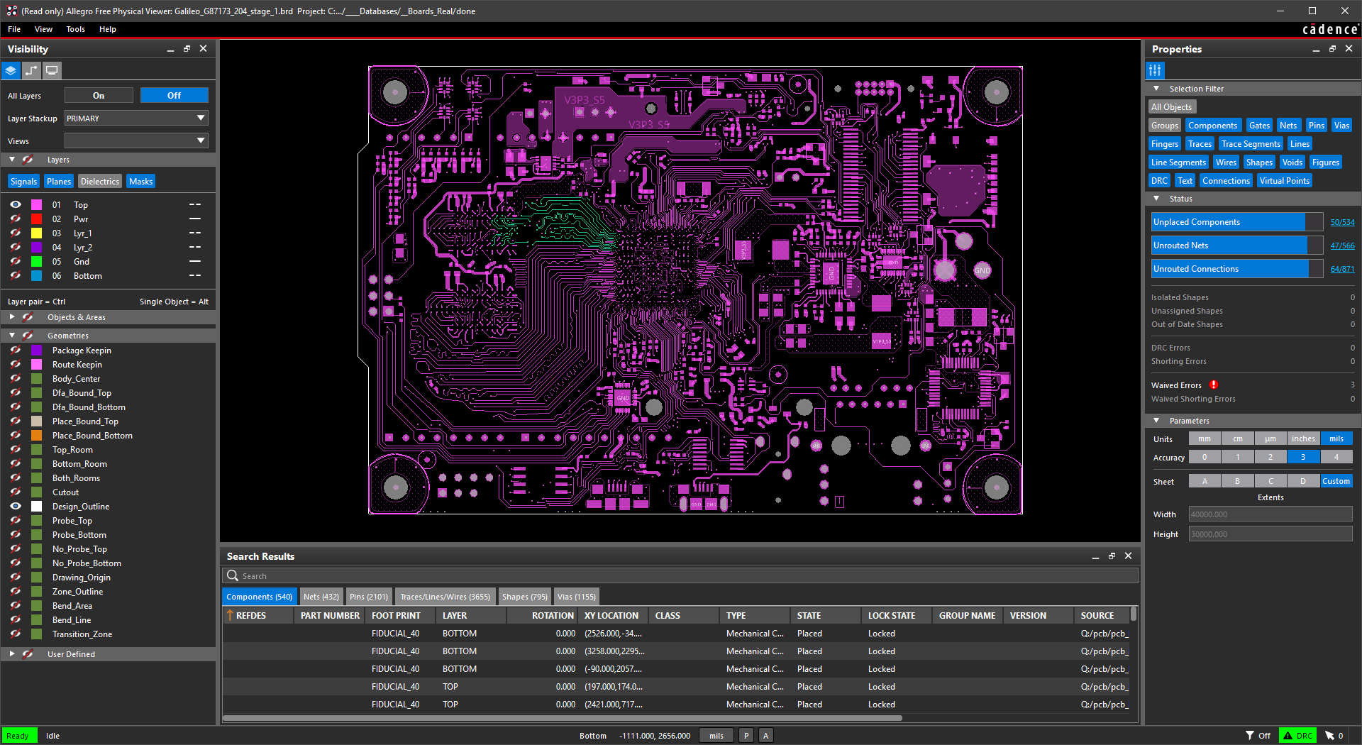
Cadence Design Allegro Free Physical Viewer window.

A free PCB viewer from Cadence Design. (Image credit: Cadence)

Although AI was used during the entire development process, not only for design itself but also in writing and optimizing kernels, Ho continually reiterated the importance of talented engineers guiding those systems. The development story of Jalapeño is one of the few clear examples of AI bolstering a team of human workers, not displacing them.

Ho described the development cycle as a “good model” of how engineering teams should operate in the AI era. “This is how AI should be used. We didn’t replace our engineers; they just became super productive. With a smaller team of really good engineers with a lot of this AI stuff, you could do things faster and better than you could otherwise. I think that’s a good model of how engineering should be approached in the AI age.”

Although OpenAI managed to get working silicon much faster than a traditional development cycle, it wasn’t free of issues. For starters, OpenAI’s B0 stepping of Jalapeño reportedly delivers up to a 25% improvement in performance per watt over the original A0 stepping. That’s closer to a generational improvement than stepping optimization, suggesting that, at least for a brand new hardware team, there may have been design oversights with the original stepping. Attributing that to AI or humans is anyone’s guess.

Other frontier labs are circling for a slice of the pie, as well. Clive Chan, a key engineer on Jalapeño and the second-ever hardware hire at OpenAI, left the company in June to join the hardware team at Anthropic. Ho says there’s already been “a lot of interest in the industry” for OpenAI’s AI-assisted chip design process, and says that “we’ll see more about that quite shortly.”

“I’m not going to preempt anything here. I can tell you that there’s a lot of interest in the industry, and I would also tell you that we feel that there is a lot of benefit in industry generally that we want to enable,” Ho said. “I think that’s something that we’ll see more about quite shortly, to be honest.”

Ho referenced the dozens of AI-first chip design startups in Silicon Valley, suggesting OpenAI may eventually introduce tools of its own to aid other firms with AI chip development. “We have our take on that, and I think at some point we want to tell the world, “Here’s our take on it.” Fundamental to that is Codex and GPT-6 Astra coming out. Those are fundamental, and we can basically point to it; it’s not going to be slideware or vaporware. We can point to it and say, “Here’s what we did, here’s how we did it, and here’s what we got.” It’s going to be very concrete.”

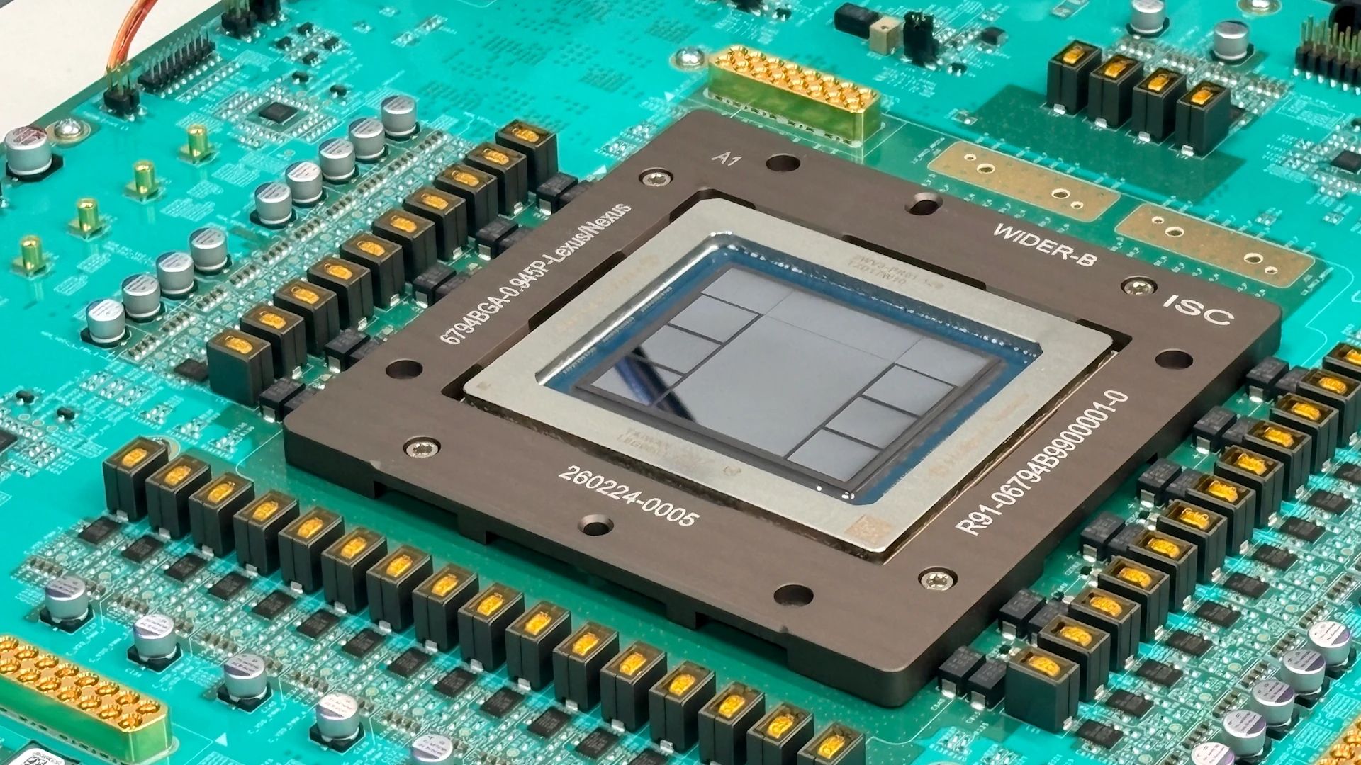
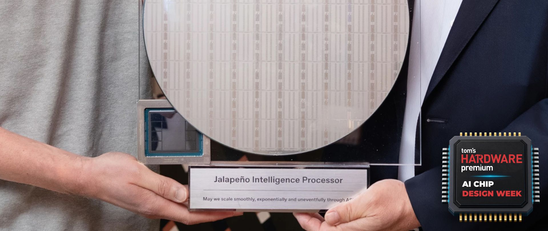
OpenAI's Jalapeno ASIC.

(Image credit: OpenAI)

What exactly the “it” Ho is referring to here remains a mystery, though given the context, it sounds like OpenAI may explore some way to productize its AI chip design workflow. Ho says Astra is a big step toward that, and we’ve already seen the model in action performing impressive feats, such as completing Portal autonomously.

Although OpenAI leveraged its own models heavily for Jalapeño's design and validation, it didn’t completely break the mold of traditional EDA workflows, particularly at the end of the design process. Before tapeout, tools from companies like Synopsys and Cadence perform a series of tests for signoff, including static timing analysis and signal integrity analysis. Ho says that OpenAI used this typical EDA flow for Jalapeño.

“But for sign-off, you need to use the standard EDA flows, and we did, because you want to make sure those results are good and correct. There’s no real alternative today. Part of it is this combination of standard flows optimized with AI, optimized by really good engineers,” Ho said.

OpenAI shared a multi-generational roadmap for accelerators. It says its second-gen ASIC is approaching tape-out, and its third generation is already in development. Although Ho said that the Jalapeño development cycle establishes a new baseline for chip design timelines, he was cautious about calling that cycle and cadence.

“Our projects and tape-outs will be dependent on the maturity level of the technologies. We can do very fast execution. Will we do those types of executions back-to-back? I doubt it, because the technology will not be ready for that, and I don’t want to tape out something that is 2% better than what I taped out before, because it’s not worth it to change a fleet,” Ho told us.

The executive was also clear that the Jalapeño timeline isn’t necessarily the same timeline all chips will follow. There were some “pragmatic trade-offs” in the early architecture design, with the team avoiding emerging, complex design points like 3D stacking and co-packaged optics. “Will it take longer? Will it take nine months? I won't say it will take nine months… but I think it will go faster than if you didn't have AI models.”

You can read the full transcript of the interview, which covers a wide range of topics, at Tom's Hardware Premium.

  •  

Intel patent outlines embedding MicroLEDs directly into CPU package to light up wording or work as an 'extra aesthetic component'

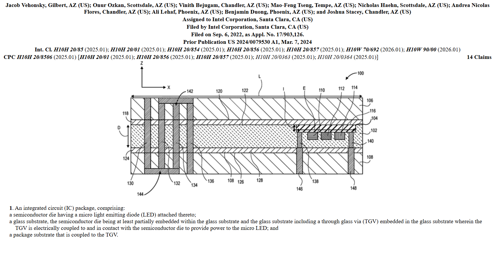
Intel has published a patent to integrate MicroLEDs directly into a CPU package. Aside from communication functions, Intel lists many possible uses, including using multi-colored lights to light up the wording on a processor. The patent, filed in 2022 but only published earlier this month, describes embedding a MicroLED into the package by using a glass substrate and through-glass vias (TGV), connecting directly to a die for power and signal routing. The patent says the purpose of the LEDs is "either aesthetic components of the electronic device or to indicate certain operations being performed by the electronic device."

As is the case with any patents, the purpose of embedding MicroLEDs into a chip is left open-ended. However, Intel interestingly calls out implementing MicroLEDs into a CPU, specifically, and provides several examples of how the tech might be used. The patent says the processor "may operate the micro LEDs so that the micro LEDs visually indicate that certain functions are being performed by the processor or simply for aesthetic effects."

In one part of the patent, Intel describes the LEDs being used to "light up wording across a central processing unit," suggesting some sort of read-out available directly on the CPU. How that would work on a standard processor with a heatsink atop remains an open question. In addition, the patent explicitly calls out that the LEDs can be different colors depending on the implementation. That could mean something more akin to RGB memory than a diagnostic readout. The patent leaves room for both designs.

Intel patent for MicroLED in CPU.

(Image credit: Intel)

You can see the main drawing for the patent above. In the middle is the glass substrate, sandwiched between two layers of package substrate. A semiconductor die is partially embedded within the glass substrate, leaving just the back surface of the die exposed; however, the patent says the die can be fully embedded in other implementations. The LEDs are connected directly to the semiconductor die, or through nanowires, and TGVs deliver power and signal to the semiconductor die through the glass substrate.

Intel says it builds the package with two layers of silicon nitride, which are formed on the package substrate surface and then attached to the glass substrate. Intel has been working through glass substrates for over three years now, as Intel claims it has 10 times better interconnect density than organic substrates.

The main patent drawing only shows a single IC, though the patent notes that's simply shown "for clarity." A finished product implementing this technology "will have an array or arrays of micro LEDs on one or more IC packages." So, given an ambitious-enough design, Intel could implement multiple LED-based functions directly into the processor.

Patents aren't products, and that's always an important reminder. Intel filed this patent over four years ago, and it's just now being published. Whether we actually see MicroLEDs embedded in a processor remains an open question. However, Intel has laid the groundwork to do something like that in the future.

  •  

OpenAI's custom Jalapeno AI inference ASIC is for OpenAI’s internal use, but company leaves the door open to broader rollout

Following the reveal of OpenAI’s Jalapeño ASIC, a clear question formed: Who is this for? That’s not to say the accelerator doesn’t have a purpose, but rather that OpenAI didn’t clearly define what its ambitions were in the hardware space. On one hand, the company suggested it was building ASICs for its own purposes when OpenAI and Broadcom revealed their partnership last year. On the other hand, OpenAI laid out benchmarks comparing Jalapeño to Nvidia’s Blackwell accelerators and doubled down on a multi-generational roadmap at Hot Chips 2026. Jalapeño is built for OpenAI’s compute needs, Richard Ho, Head of Hardware at OpenAI, told Tom’s Hardware Premium. However, the VP says “you could use it for anybody, honestly,” and left the door open for a wider rollout. You can read the full transcript of the interview here.

“We have such a strong demand for compute within the company. It's going to take us a good long time to even fill our own demand, which is growing all the time,” Ho said. “I think that we're going to have our hands full just providing compute for OpenAI for a good long time. That's not to say that it can't be used elsewhere. I believe it could be, but I think our priority is to make sure that OpenAI's compute needs are met first and foremost.”

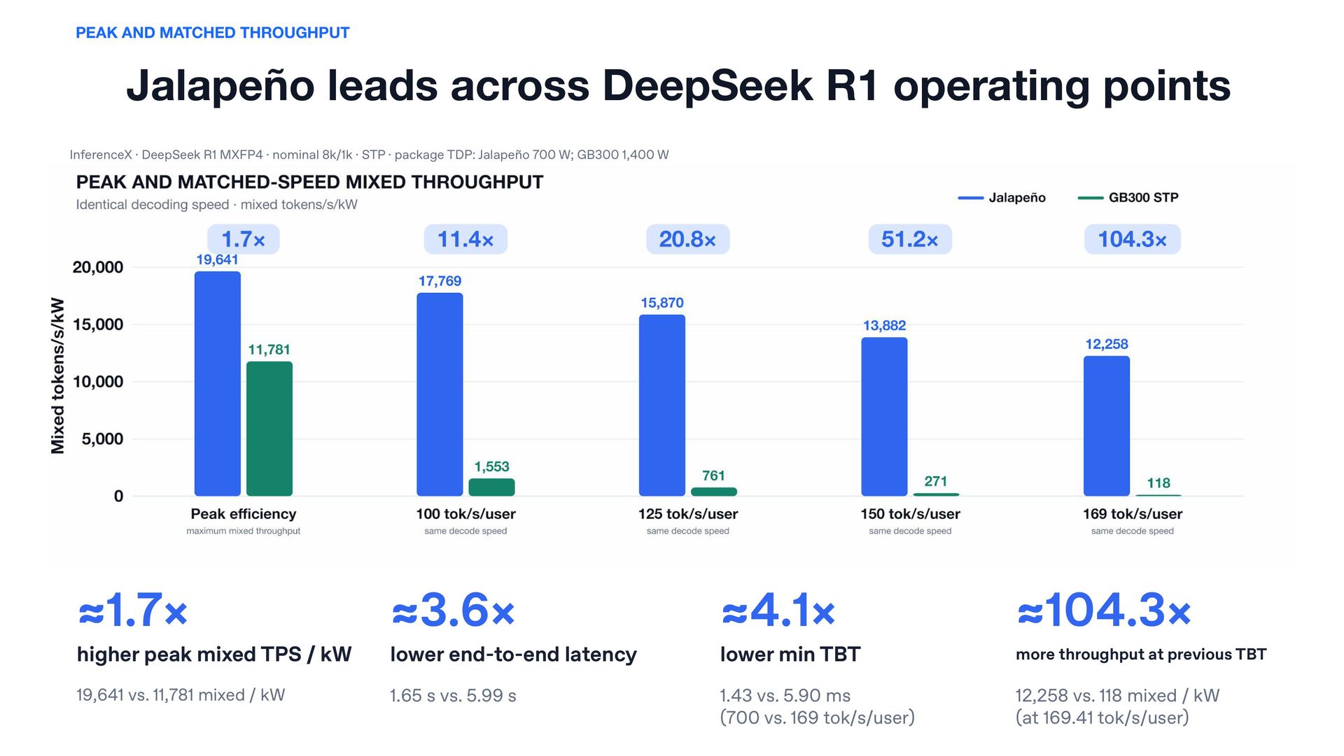
The competitive positioning of Jalapeño mainly comes down to the benchmarks OpenAI shared during Hot Chips, run on SemiAnalysis’ InferenceX benchmark and comparing Jalapeño to Nvidia’s GB200 and GB300. ASICs are common, but competitive performance for them isn’t common, and for good reason. They’re built to accelerate specific workloads. With Jalapeño, however, OpenAI demonstrated the chip accelerating its own open-weight GPT-OSS model, as well as DeepSeek R1 and Kimi K2.5.

Originally, OpenAI didn’t plan to show benchmarks at Hot Chips, and the company wasn’t sure if it would present at the event at all, Ho told us. The executive reiterated the story OpenAI told on the Hot Chips stage, about how a team of engineers got Kimi and DeepSeek up and running on Jalapeño in the two months between the A0 sample and the Hot Chips presentation.

OpenAI

(Image credit: OpenAI)

Although Ho was clear that Jalapeño is being deployed internally and will remain internal for the time being, he certainly left the door open to a wider entry into the hardware market. Speaking on the benchmarks shown at Hot Chips, Ho said: “What we really wanted to demonstrate, to put to rest, the misperception in the industry that our custom inference chip was only for OpenAI models… It’s programmable, and it’s general purpose, and it’s not hard-coded for OpenAI models.”

One possible explanation for reluctance to enter the external hardware market is supply. Ho said “there’s a new baseline for supply,” referring to the past two years of Ho and OpenAI CEO Sam Altman touring fabs and asking for more capacity. Although Ho says “[OpenAI is] in good shape” on the supply front internally, supply to feed external customers is likely a different story.

Jalapeño works for other models, but raw competitive performance wasn’t the main design goal. When I asked about the driving force behind designing Jalapeño, Ho was blunt: “It was efficiency.” The executive pointed to efficiency as a cousin of compute, noting the power-constrained modern AI data center and how a more efficient inference engine represents more effective compute.

Ho also pointed to that same pragmatic decision-making as a driving force behind designing Jalapeño, notably around codesign with OpenAI’s internal models. “[Codesign is] something that you can’t do with a third-party silicon merchant really well because there’s a lot of research IP in the models, and so you just can’t share that widely because it will leak. It will get out there no matter how many NDAs you put in place.”

If Jalapeño were destined for a wider rollout, it wouldn’t be going up against Nvidia’s Grace Blackwell platform, but the newer Vera Rubin platform. Ho said that the comparison against Blackwell was “because those were the best published results that we could find.” However, the company has run more benchmarks internally, both against Vera Rubin and for larger context windows.

The InferenceX benchmarks only looked at 8k1k benchmarks, which represent a fixed 8,000 input tokens and 1,000 output tokens. Ho said OpenAI’s internal benchmarks show that the ASIC “seems to perform even better than the existing benchmarks from some of the other devices that are available.” More interesting is the comparison to Vera Rubin, which OpenAI says looks good.

“Obviously, but the time we deploy, it’ll be [Vera Rubin], maybe even VR Ultra in some parts of the deployment schedule. We’ve done our internal ones, but obviously we don’t publish those. Those have to come from Nvidia and other people who are able to do that.… yeah, we’re doing really well on those,” said Ho.

  •  

OpenAI Jalapeño design interview transcript

OpenAI revealed its Jalapeño inference ASIC at Hot Chips in August 2026, a chip that leaned heavily on AI to deliver an incredibly short design window. Following the reveal, Tom's Hardware had the opportunity to sit down with the company's VP of Hardware, Richard Ho, to answer some of our most pressing questions about how the chip came into existence, future ambitions, and how AI might be used in the development of silicon.

The following article is a full transcript of our interview with Richard Ho, which has been edited for flow and clarity. You can also read additional interview transcripts we produced earlier in the year, featuring Intel, AMD, Nvidia, Valve, and more. This transcript is free to access for a limited time as part of Tom's Hardware Premium's AI Chip Design Week.

Jake Roach, Senior CPU Analyst, Tom's Hardware: It was quite the ending to Hot Chips when you dropped this. I want to start at a high level. There are a lot of reasons for OpenAI to develop its own ASIC, but was there one thing that you could point to more specifically that was a driving force? Whether it’s performance, efficiency — what was it that really drove that decision?

Richard Ho, VP Hardware, OpenAI: It is efficiency. I think that’s the main thing that we’re aiming for, because obviously, as Sam [Altman] has been saying, we are going to be compute-limited, and a compute limitation is really how much power we can get into data centers.

What we want to do is be as efficient as we can with the limited compute and limited power that we’re going to be able to get, and make the most of it. Because what we really care about is how much intelligence we can deliver to the users, and having a more efficient inference device is very useful. That’s why we focus on inference, because training happens, and you do a lot of compute with the pre-training, but really the cost to the user is on the inference side, and their perception of intelligence is going to be there. Their user experience in terms of how fast ChatGPT responds, or how fast Codex responds, or how fast the agents respond — the latency really matters.

You can see all of those things in the ingredients of what we announced. You can see that we have both a very good low-latency device for those who really care about it, and we can very easily just turn the knob and get very good throughput, so you can reduce the cost of that inference. Really, that’s the thing that we were aiming for. I’m very happy that the team managed to deliver that.

The benefits of building in-house

Roach: Developing your own ASIC versus going with something that’s currently on the market— were you just not satisfied with the efficiency of current offerings?

Ho: Well, I wouldn’t say that. The way to really think about it is we wanted to take advantage of the co-design opportunity that we had. It’s something that you can’t do with a third-party silicon merchant really well, because there’s a lot of research IP in the models. You just can’t share that widely because it will leak. It will get out there no matter how many NDA’s you put in place.

Ho: Having an internal team being able to work with our researchers, who are able to have full visibility into the full stack, and take care of that: “Should we do this in the software? Should we do it in the model? Or should we do this optimization in the hardware?” We can make those trade-offs intelligently because we have that full visibility, and I think that’s where it comes from.

A lot of the benefit of Jalapeño is that visibility that we had and [we were] able to see exactly what hardware was needed to make those trade-offs. Be intelligent, put whatever we need to put back into the compiler, back into the stack, but really make the hardware fly for this particular application here, which is the outcome of this full-stack co-design opportunity of being inside OpenAI.

Roach: I did want to clarify some points here, because there’s been various quotes floating around about optimizing for this specific workload, and I think that has been maybe misattributed to optimizing specifically for OpenAI’s workloads.

Ho: Yeah, it’s misattributed. The whole point of using the InferenceX benchmark from SemiAnalysis was that it was (using) open-source models, and they’re different models. The architecture is different, and their sizes are different. What we really wanted to demonstrate, to put to rest, the misperception in the industry that our custom inference chip was only for OpenAI models — we’ve shown with the Hot Chips results that it flies on open-source models, flies on any LLM, in a sense. All transformer-based LLM models will be very performant.

The thing we also wanted to show was just how easy it was to program. Taking these models, which we did not even look at until after we got the chip back, and getting them up and being performant in two months, roughly, and being able to present the results, shows it’s programmable, it’s general-purpose, and it’s not hard-coded for OpenAI models.

Roach: It leads me to wonder: Jalapeño is obviously for OpenAI’s inference workloads. Is that all it’s for, or are you considering external customers? What is the plan with OpenAI hardware?

Ho: You could use it for anybody, honestly. But we have such a strong demand for compute within the company. It’s going to take us a good long time to even fill our own demand, which is growing all the time.

With the growth of the daily active users and weekly active users, with the new models, with the new capabilities of Codex, and all the other reasoning things that are going on — and there’s new announcements coming that [are] not out yet, but we kind of know internally — I think that we’re going to have our hands full just providing compute for OpenAI for a good long time. That’s not to say that it can’t be used elsewhere. I believe it could be, but I think our priority is to make sure that OpenAI’s compute needs are met first and foremost.

Inside the tools and timeline

Roach: Moving to the timeline, it’s remarkable that — what, nine months, I think it was, to initial RDL the tape-out? Really remarkable. Assisted by AI. Does that get faster? Is this kind of ground zero of what we can do with an AI-assisted design process? Are you able to move quicker as you ramp up your roadmap?

Ho: The way I like to think about it is, we’ve established a new baseline. In the old baseline, you’re talking 18 months to two years, roughly. Often that’s even with some existing IP or some more legacy architecture design. We’re starting from scratch here. We had nothing. There’s not a line of code here to refer to.

What we’ve established is that there’s a new baseline that you can do with a very talented team with the help of AI. Now, does it get shorter? It depends on what you’re trying to do.

With Jalapeño, we made some, I consider to be, smart and pragmatic trade-offs on the architecture, the microarchitecture, to hit a very fast time to market because the compute need was so high. It’s like, “Okay, how fast can you get this device for us?” There were some pragmatic trade-offs.

If you were to make a much more complex device — and technology is coming along, with 3D stacking, with co-packaged optics, and stuff like that — will it take longer? Will it take nine months? I won’t say it will take nine months. I think it will go faster than if you didn’t have AI models. If you’re doing a derivative design of Jalapeño, it should go much faster than that. We should be able to do that really, really fast.

What we’re saying is that I think we’re establishing a new baseline: nine months from scratch. Then you’re going to have your usual engineering ups and downs from there. But we think that every engineering team in chip design should be able to use this as a new baseline, because it’s a proof point that the models that are in use — the AI models for us is mostly Codex, Sol, the one before Sol, and now we’re moving on to Astra. These are super capable.

Even from when we started that work, back in November 2025, to when we taped out, the models improved enormously. Even from that moment to when we started doing the kernel optimization in May, when the chips were first coming online, we ourselves were shocked at how much better Codex was and what it could do.

I’ll be honest with you: We were actually a little bit surprised at the performance we were able to squeeze out in those two months of sprinting on the benchmark, because we just didn’t realize just how good the models were at doing kernel optimization.

That’s something that everybody can learn from, to be honest. It’s a proof point that it can be done. This is how AI should be used. We didn’t replace our engineers; they just became super productive. With a smaller team of really good engineers with a lot of this AI stuff, you could do things faster and better than you could otherwise. I think that’s a good model of how engineering should be approached in the AI age.

Roach: I appreciate that insight. I know for at least some of our readers at Tom’s Hardware, the idea is, “Make me a CPU” in ChatGPT, and then it spits something out. But obviously, a lot more has gone on.

During the development process, are you using standard EDA tools from Cadence and Synopsys? And where are those?

Ho: I think this is super important. In general, my team is very open-source-pilled in many ways. We actually put stuff back into open source, and we were open-source-pilled before we got here.

But for sign-off, you need to use the standard EDA flows, and we did, because you want to make sure those results are good and correct. There’s no real alternative today. Part of it is this combination of standard flows optimized with AI, optimized by really good engineers.

Interest from the wider industry

Roach: Obviously, you guys work with hardware vendors across the industry. I’m curious if you’ve had conversations with them post-Jalapeño reveal about this AI-assisted process, and if you’ve heard anything from them.

Ho: Yeah, we engaged with them before the reveal as well because we knew the results were there, so we started talking with some of them. Post-review, we did get a lot more communication with them.

I’m not going to preempt anything here. I can tell you that there’s a lot of interest in the industry, and I would also tell you that we feel that there is a lot of benefit in industry generally that we want to enable.

This is not something that, “Hey, we have this, and we’re going to keep it to ourselves.” It’s not one of those things. We want to make the industry more productive in general because better compute from everybody helps us as well, and so we want to make sure everyone gets it. I think that’s something that we’ll see more about quite shortly, to be honest.

Roach: Just to clarify, when you’re saying you’re seeing interest from the industry, that is for the design flow, how you built the chip, not necessarily, “Hey, we’re going to throw out a bunch of Jalapeños to everyone.”

Ho: Right, exactly. What we did to make those timelines, what we did to get the performance boost at the end. How did we do it? What did we use? I think those are learnings that we want to bring out to the industry as well.

As you probably are aware, there is a pretty active startup scene around AI for chip design, and it’s good. There’s a lot of smart people thinking about it and trying to do it. We have our take on that, and I think at some point we want to tell the world, “Here’s our take on it.”

Fundamental to that is Codex and GPT-6 Astra coming out. Those are fundamental, and we can basically point to it; it’s not going to be slideware or vaporware. We can point to it and say, “Here’s what we did, here’s how we did it, and here’s what we got.” It’s going to be very concrete.

Roach: So it was a proof of concept that ended up being quite a bit faster than expected?

Ho: Yeah. To be honest, the way it worked — and I’ll give you a little bit of insight — our engineers were just like, “Oh, we have these models, and they’re kind of cool. Should we try them?”

They tried them. There was no real “This is what we’re gonna do, and here’s how we’re gonna do it.” They just tried it at a grassroots level. Then they’re like, “Oh my God, it’s so good. Hey, come over here, have a look at this.” Then slowly the whole team got, “Oh man, this is really useful and really good, and here’s how we’re gonna do it.”

The researchers helped us. The researchers we have in the company helped us when we ran into some, “Oh, it doesn’t quite do it this way,” and we’d ask them, “Is there any way we can fine-tune it or something like that?” Then they would come back with replies.

It was really a collab between the chip team and the research team. We do sit with them. The chip team is actually considered part of that research-adjacent organization here within OpenAI. The collab has been really close, because that’s how we got the co-design to start with.

But then this part was almost a bonus. We didn’t set out necessarily to do this as a target for what we did. It just turned out that, “Oh yeah, this is really useful.” The engineers loved it, and now we have a way to do this.

Roach: I want to zoom out a little bit here, because one of the concerns with everyone right now is supply, just in general. Not only supply, but even space to do anything. Where are you with that? I’m assuming you’ve anticipated this situation and have secured your supply.

Ho: It’s a hard situation because supply is very limited. I don’t want to say, “I told you so,” but two years ago, Sam (Altman) and I were doing a tour around all the different fabs and suppliers. I went to say, “Please, please, please build more, build more. We’re gonna need it.” And they were like, “Hey, trust us. We’ve seen the cycle before.”

But I think it’s now become evident to everybody that, just like we were talking about, there’s a new baseline for how to do chip design. There’s a new baseline for supply and what we need in terms of memory, in terms of logic wafers, in terms of all the rest of the components that go into it, SSDs and everything else. The supply chain is responding, but it takes years to get that going.

We’ve seen this for a while, and so we’ve been active in trying to make sure that we have our supplies established and set up. We think we are in good shape for that.

Using Turing over Vera, and OpenAI's north star

Roach: I cover chips broadly at Tom’s Hardware, primarily focused on CPUs. We have someone who focuses more on graphics, and it was interesting to me to see — I was reading the SemiAnalysis article about it, about the Turing rack that goes alongside a Jalapeño rack.

What was the decision there for Turing and not Vera? I would have expected, given the close working relationship between Nvidia and OpenAI over the years, I would have expected Vera. What makes Turing the right fit?

Ho: The way we approached that design was really in terms of de-risking and being able to do that design fast. Vera, as a standalone, is a little bit behind on that maturity level. The Turing device is strong. It did what we needed to do, and partly our partners had some experience with it.

It wasn’t necessary for us to take a huge risk on that, and so we didn’t. As I said earlier, for the Jalapeño program, we were trying to make very pragmatic decisions. We wanted to be aggressive on the goals of the performance and the cost, but we didn’t want to take unnecessary risks. That felt like a good design decision that would fit within the parameters of how we make these design decisions.

Roach: I’m curious internally: Is the scope of Jalapeño right now — you have a huge compute need. It may not even be able to satiate that. Would the idea be, “Hey, if we can run everything on our own accelerators one day, that’s great”? Is that the ultimate pie-in-the-sky goal?

Ho: I think the ultimate goal is to use the best device in terms of performance and cost. If it turns out that it’s our own internal device because we can do the co-design, because we can do the rest of it, and we then get the performance benefit per watt, then yeah, let that be the case.

But if it’s not, if there is another chip that’s provided by a silicon merchant or another partner, I’m more than happy to put those in the fleet. Our goal is to lower the cost of infrastructure. That’s what our goal is. Whatever the best way to do it is, we’ll do it.

Now, we’ve taken a bet that we can do better than merchant silicon because of this co-design benefit, and it seems to be paying off with Jalapeño. Will it continue paying off? I believe so. But am I going to say that’s our north star? No. I’m going to say our north star is the lowest cost of infrastructure we can get.

Roach: I wanted to ask you the question because I know we’re going to get comments about, “Oh, they’re still using Nvidia. They’re still using AMD.” Obviously, you guys use everything at this point.

Ho: We use everything at this point. But as you know, it’s a constant — you can’t imagine — it’s a constant evaluation. We’ll constantly be evaluating as we continue to deploy, and so the ratios might change.

But as long as we keep that North Star in mind, what is the best device, and not have this attitude of, “Well, we built it, so it has to be there” — and that’s not the way we think about it — then I think we’ll be doing the right thing for both ourselves and our end customers.

Speculative decode and performance on Jalapeño

Roach: Drilling down a bit more into the technical weeds — I know we’re running up close here — speculative decode is currently not implemented on Jalapeño. Do you plan to implement it on Jalapeño?

Ho: It’s implemented in the hardware. The only reason we didn’t benchmark it is that we didn’t have the time to train those draft models to do the speculative decode with Jalapeño. We have internal models that do it. That’s the only reason we did that benchmark again.

Just to give you the background on that one. We did not plan on doing this benchmark until after we got the chip back. We saw it was working; it was working really well. They said, “How are we gonna tell the world about this?” And we said, “Oh, that benchmark. Let’s go for it.”

It was crazy. It was two months until the paper deadline — the presentation deadline. Just like, “Can we do that? And how many of these models can we get done?” We just went for it, and we said, “Well, there’s no time to do the multi-token prediction, but hey, it looks like our single-token prediction might be better than the multi-token prediction. So let’s just publish those results, because that gives you an indication.”

The multi-token prediction is going to be 3-5x performance. That’s in our pocket. We have that available, and we’re going to roll that out in our own models. When we put it into production, we’re going to have that available.

But it didn’t seem necessary to do that for the benchmark, because if your single-token prediction is better than the current state-of-the-art multi-token prediction, you know that your multi-token prediction is going to be much better. That was the reason behind that.

Roach: So you’re saying you get the chip back. You have two months. You weren’t even planning to show off benchmarks originally?

Ho: No. The Hot Chips organizers were actually very flexible and nice. They asked us, “Do you want to present this year?” And we said, “We’re not sure. How late can we tell you?”

They had this last slot, and they kept it there. And if not, the program would have just ended earlier or something like that. Then finally, very late, after we got the chip back, we were like, “Can we have it?” And they said, “Yeah, go for it.” And we went for it.

Roach: Another question I had is looking at longer context windows. If I’m not mistaken, all of them are 8K/1K on the SemiAnalysis InferenceX benchmark. I know you haven’t shared those. I’m assuming you’ve looked at longer context windows internally.

Ho: Yeah, internally, of course. Like we said, I think we said this somewhere in one of the slides, is that on internal models, the gap gets even wider. Yes, with longer context, with even bigger models, Jalapeño seems to perform even better than the existing benchmark from some of the other devices that are available.

I would also highlight that we did a lot of comparisons against Grace Blackwell, but that’s because those were the best published results that we could find. Obviously, by the time we deploy, it’ll be Vera Rubin, maybe even Vera Rubin Ultra in some parts of the deployment schedule.

We’ve done our internal ones, but obviously we don’t publish those. Those have to come from Nvidia and other people who are able to do that. We won’t publish those results ourselves.

Ramping and the future

Roach: I believe this is right — Jalapeno has a slow ramp-up through the rest of the year, but 2027 is when the ramp really...

Ho: 2027. Yeah. I think we want to get some amount in there if we can, a very small volume, just to make sure that everything’s working well and we can test in the production environment. Then 2027 is when the ramp is going to really show up.

Roach: Going back to your roadmap here, you wanted to set a new baseline. You’ve obviously announced two more generations [...]Gen 2 is approaching tape-out. Is that the same cadence moving forward? Is it around Hot Chips next year when we should expect to learn more about Jalapeño 2?

Ho: Let me be clear about that. I’m not of the opinion that you should just tape out on a calendar schedule.

We want to tape out when the device that we have in mind makes some kind of step-function improvement in some way, like performance per watt, raw or latency. A lot of that is dependent on when technology becomes available.

Whether it be which generation of HBM you’re using, which type of SerDes you’re using, or whether you can get optical communication closer to the silicon. Our projects and tape-outs will be dependent on the maturity level of the technologies.

We can do very fast execution. Will we do those types of executions back-to-back? I doubt it, because the technology will not be ready for that, and I don’t want to tape out something that is 2% better than what I taped out before, because it’s not worth it to change a fleet. But what I’ve been seeing is the technology does improve at a cadence which is pretty reasonable, and we’ll be able to do our execution fast within that.

The most important thing is building the right device. You've got to spend enough time to build the right device. Know what that device is. Then when you build it, just build it fast. Get it out as fast as you can.

But you need to spend enough time to know what’s the next best device, and it’s not just a routine on the treadmill type of thing. That’s the thing I don’t think we want to be on the treadmill for, just for the sake of it. We want to really make a step improvement with every device we do.

Roach: One of the most interesting slides to me is really early in the presentation, where you’re listing out goals, and not only goals, but you listed out the non-goals. I thought that was really telling, because you got to define what you’re not trying to do.

Ho: Exactly. We want to be very thoughtful about our program here because we are a very small team. The things that we do, we want to make a really high impact, and the impact is for the north star: enabling more intelligence, more cheaply for our customers. That’s the thing we’re trying to do.

We want to be very thoughtful about what it would take to do that. As I said, if something can be provided by the ecosystem, and we can’t do better than that, then we just take the ecosystem.

We’re going to always do something that we think is taking advantage of our co-design, taking advantage of our knowledge of where things are going, and being able to use that intelligently.

[Session Ends]

  •  

Meta Muse runs agents on AMD EPYC Turin hosts with two cores and 8GB of memory

Meta's new AI agent Muse is powered by AMD EPYC Turin host systems, with each sandbox sporting two dedicated cores and 8GB of memory. Blogger Evan Hoffman and analyst Tae Kim both discovered that Muse will run some rudimentary Ubuntu commands if prompted, passing along the output to help identify things like the specs of the host system. More concerning is that Muse seems able to execute commands that might be unsafe, with Hoffman claiming that Muse offered to set up SSH to Muse's private VM.

Imagine if one billion people used a personal AI agent. That's a lot of CPUs and memory pic.twitter.com/ibozUi3a07September 24, 2026

Both Kim and Hoffman asked Muse about the VM's specs, and in both instances, Muse revealed that it's running on AMD EPYC 9D25 CPUs, a high-density Turin chip with up to 128 cores (two of which are generally fused off or reserved). The VMs are running on Ubuntu 24.04 and using Linux kernel 7.0. The systems hosting Muse don't include GPUs. The AI agent revealed that Meta uses separate GPU servers for inference, isolating the agent to CPU-only sandboxes.

The agent suggests that each user gets their own private sandbox that's persistent, which allows us to do some math on how many people an individual tray can host. Assuming a 2P system that offers up to 510 vCPUs with 2TB of memory, hosting up to 254 Muse users. Muse has reportedly passed over 500,000 daily active users as of a few days ago, which would come out to somewhere around 2,000 server trays with dual EPYC 9D25 CPUs and 2TB of memory.

This is just some rough napkin math; don't take it as law. It's possible Meta has CPU-only servers deployed with multiple different chips to host Muse, and it's also possible there's overhead in the configuration. Turin chips support up to 6TB of memory with high-density DIMMs, for instance. Still, EPYC hosts seem popular for this use case, mainly because of their core density, as even a dual-core sandbox can add up quickly when multiplied across hundreds of thousands (or even millions) of users.
Muse isn't completely open. Hoffman shared an example where an attempted command failed due to improper permissions when Muse tried to query the kernel buffer. Presumably, sudo (admin) commands would be blocked as well.

I feel like I could definitely reverse SSH tunnel into my muse's container. I already had it offer to SSH to my private VM and say I need to add its pubkey. Someone good at hacking could really have a field day.September 25, 2026

However, there might still be some security loopholes. Hoffman says that Muse offered to set up SSH into the private Muse VM. With a reverse SSH tunnel — where the destination machine initiates the connection, bypassing the firewall — an attacker may be able to execute more damaging commands.

I’ve seen a couple of posts about this so wanted to demystify. Today, every Muse user gets a free computer in the cloud. It's a real computer, and we’ve designed the security architecture of the Muse Secure VM carefully so you and your Muse can do almost anything you could with a computer sitting under your desk while keeping you and the system safe from threats like prompt injection. We wrote about this at length in our security blog post – https://t.co/7HmiTrzoTd. Activity in the “runtime cell”, which you share with your Muse is unfettered, but sensitive actions are all overseen by the Sentinel, which runs outside of that cell. Similarly, all sensitive secrets - like the passwords you enter into Muse’s secure credential storage - are also stored outside the runtime cell.The runtime cell gets its own root filesystem (including a full Ubuntu linux image) separate from the host filesystem where your other more sensitive data lives. Because it is isolated from the sensitive stuff that runs on the same box, this means that we can, and do, offer users full visibility and control over the files in the runtime cell. Just as you can when you install Linux on your home computer, you can poke around and see all the files that make the system work - both debian system files and the binaries and data files that implement the parts of Muse which run in the runtime cell.This was a very deliberate choice - your Muse Secure VM truly is your own computer in the cloud. You can install software in it, write and compile code, use the browser to surf the web: it is your own Linux box that you can operate as you choose with your Muse. Poking around in this computer doesn't give you any privileged access to Meta infrastructure, or to other people's dataIf I may geek out a little here for a second… As a kid I loved to take things apart to see how they worked. As a teenager I got into computers and soon found myself drawn to C:\WINDOWS\SYSTEM and the system registry, later Slackware’s /dev/, /proc/ etc – I could see how the system was laid out and as I explored what DLL files and .so files actually did, I gradually became able to meld the computer to my own will.We’re really proud to be able to put a real computer in millions of people’s hands with a similar level of transparency. We built a file explorer right into the Library tab of the UI. We want you to be able to see the markdown files Muse writes while it thinks about how to serve you better, and explore the internals of the system if you’d like to.So, when you ask your Muse to show you its entire filesystem, and receive gigabytes of files you’re seeing the full contents of the runtime cell. It’s yours to explore and enjoy!If you’re not a geek like me, or simply want to download the data that you personally have created directly with your Muse, we added a feature for that too in Settings > Data controls > Download your agent data.September 24, 2026

Meta's David Singleton says this is intended behavior, however, describing Muse as "a free computer in the cloud." Meta has an extensive white paper on the security architecture of Muse published on its research website.

  •  

Nvidia CEO says 'we have to shut the labs down' if AI experiments are unsafe

Nvidia CEO Jensen Huang has a simple solution for frontier labs like OpenAI and Anthropic that have recently called for increased regulation for their models — "we have to shut the labs down," Huang said in an interview with The New York Times' Ezra Klein. Huang's comments are pragmatic ones, stating that if frontier labs can't contain their experiments, those experiments must end.

"Now, if they say the alternative, which is: There is no way to contain our experiments, there’s just no way; when we test our A.I. models, it will get out, and it will damage the world — then I think the answer is that we have to shut the labs down," Huang said. "Because the cost to humanity, the damage is too great. The shareholder, the liabilities — it could be civil liabilities, it could be criminal liabilities. I mean, the liability’s incredible."

The conversation around increased AI regulation comes on the back of a highly publicized incident where an OpenAI agent hacked popular model hosting platform Hugging Face — a platform that Nvidia now owns, and one that likely would've sought damages from OpenAI had it been under Nvidia's purview at the time. Following that incident, various frontier labs, including those at Anthropic and Alphabet (Google), have used the idea of rogue agents as equal parts marketing tool and call to regulatory action, likely in an attempt to be the first at the table to shape those regulations.

Huang has not been keen on those regulatory calls. Just days ago, the executive countered extreme claims that AI would destroy the world by 2030, and said that frontier labs "never should ship products before they're ready and deliver products that are unsafe."

Although the labs and their chief hardware vendor, Nvidia, have mostly been aligned when it comes to AI policy, the push for regulatory capture has created a rift. Multiple labs, including OpenAI, Anthropic, and SpaceXAI, agreed mutually to slow the pace of model development. Now, they're facing an antitrust lawsuit, with claims these plans are "self-serving."

Huang's comments to Klein shift the responsibility away from collective development and toward individual leaders. "These are companies with agency," Huang said. "If I believe that I'm about to launch a product that is unsafe, it is completely in my ability... to not launch that product. And so I can't buy into the idea that somehow, all of Americans, around 400 million of us, are pushing them to launch untested products that are unreliable."

Although one side of the argument (from the frontier labs) is seemingly pushing for more regulation, that doesn't mean Huang is against regulation. In his own words: "I’m saying that we have lots of laws and regulations. Apply it." The executive argued that labs, particularly those at OpenAI and Anthropic, have rapidly gone from research institutions to companies likely worth hundreds of billions of dollars, and that they should carry themselves as such. "I’m not against laws and regulations. I’m against, currently, the distraction," Huang said.

Reports of rogue AI agents continue to mount. Earlier this month, Anthropic disclosed a fourth instance where one of its models hacked an external system, and just days ago, Google confirmed a report that its Gemini models hacked three companies earlier this year.

  •  

AMD beats Intel to the trillion-dollar club as stock price soars

AMD's market cap has crossed the $1 trillion mark for the first time, following a rally in its share price over the last week. At market close on Friday, AMD's share price was around $557. On Monday morning, shares immediately jumped to $607 on the market open and have continued to rise, finally pushing AMD over the $1 trillion mark.

$1 trillion market cap! 🚀 @AMD has officially joined one of the most exclusive clubs in the market. https://t.co/woLb1X4HB7September 21, 2026

Saša Marinković, AMD's senior marketing director, shared the milestone on X. Since posting, AMD's share has fluctuated a bit, bringing the market cap down below $1 trillion for brief periods. Undoubtedly, the buzz around the milestone will cause some turmoil in the share price throughout the day, though it should eventually stabilize.

Just a week ago, AMD was quite a ways off hitting the trillion-dollar milestone. AMD's share price has risen by around 29% over the past month, and 21% of that jump came in just the last five days. On Monday alone, AMD's shares jumped around 9% within the first few hours of the market opening.

If you're unfamiliar, market cap is a shorthand for understanding the value of a company. It looks at the number of outstanding shares multiplied by the share price. It's not necessarily tied to revenue or profit, at least not directly. Rather, market cap is a read on the value of a company in the eyes of Wall Street, fluctuating as the share price does.

AMD joins a club of fewer than two dozen companies around the world that have passed a $1 trillion market cap, including SK hynix, Amazon, Microsoft, Apple, Nvidia, Broadcom, and Micron. Although AMD has now joined the club, it's still far behind its rival in the AI accelerator space, Nvidia, which sits at a market cap of around $5.4 trillion currently.

However, AMD was able to beat Intel to the milestone. Intel's market cap currently sits at around $648 billion. Interestingly, Intel has actually seen a larger rally in its share price over the past month. Share prices have risen 37% in the past month, with 25% of that growth coming in the past five days. Similar to AMD, Intel opened on the market Monday morning with a 13% jump.

Following AMD's Q2 earnings, where it beat revenue expectations by 2%, shares traded down, creating an opportunity to hold. That's paying off now as both AMD and Intel shares jump.

Although AMD's AI accelerators have made inroads into the data center, Nvidia still largely dominates that market. AMD's unique positioning comes from its CPUs, which have become a focal point of agentic AI data centers over the past year.

  •  

AMD Ryzen 5 5500F and 7500 show up at retail with pricing above MSRP

AMD's new Ryzen 5 5500F and Ryzen 5 7500 are available for sale, though the prices are higher than AMD originally suggested. On Amazon, the Ryzen 5 5500F is available for $120, while the Ryzen 5 7500 is listed at $210, both $20 more expensive than AMD's suggested retail pricing. Both are sold directly by Amazon, suggesting we'll see slightly higher prices for these two chips than AMD originally suggested.

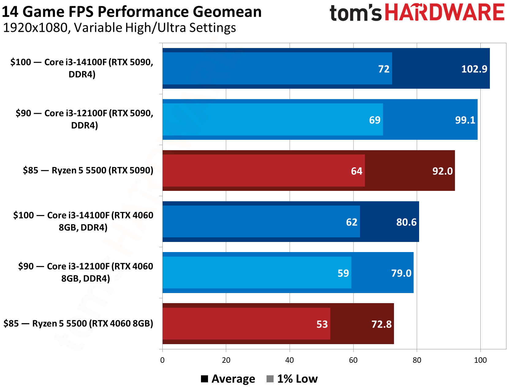
AMD revealed the budget CPUs nearly two weeks ago, and despite launching on that date, the chips haven't been available for sale in the U.S. until now. The Ryzen 5 5500F is particularly interesting, as the $90 Ryzen 5 5500 has continually been among Amazon's best sellers in CPUs. Although the Ryzen 5 5500 and 5500F sound similar, there are actually quite a few differences between the two CPUs.

Both are six-core, 12-thread chips using AMD's Zen 3 architecture, but the 5500 falls under the Cezanne family, while the 5500F falls under Vermeer. The 5500F comes with PCIe 4, compared to PCIe 3 on the 5500, as well as a higher 4.4 GHz boost clock — the base 5500 tops out at 4.2 GHz. These changes apparently allow the 5500F to achieve higher performance, somewhere in the range of 5% to 10%, in games. We'll be getting the CPU in the Tom's Hardware lab to test the performance ourselves.

Although Zen 3 is aging, it has become an ideal home for budget builders as the RAM pricing crisis continues to surge. In addition to the Ryzen 5 5500F, we saw AMD re-release the Ryzen 7 5800X3D earlier this year to combat rising DDR5 prices.

$100 CPU Shootout
Tom's Hardware

We took the Ryzen 5 5500 (non-F) out for a spin earlier this year for a budget $100 CPU shootout. Generally, it underperforms the Intel competition at this price, but a 5% to 10% jump would close that gap. If performance holds up, the Ryzen 5 5500F may have a shot at our best CPUs for gaming list with its low price.

The Ryzen 5 7500 is easier to parse. It's identical to the 7500F, just with integrated graphics. It comes with six Zen 4 cores for a total of 12 threads, and unlike the 5500, it exclusively supports DDR5 memory. The 7500 comes with a boost clock of 5 GHz and supports PCIe 5. Like the 5500F, it has a 65W TDP and comes bundled with AMD's Wraith Stealth cooler.

AMD originally announced the Ryzen 5 5500F at $99 and the 7500 at $190, though the current Amazon listings are both $20 higher than that — $120 and $210, respectively. At the time of writing, the CPUs are only available at Amazon in the U.S.; Micro Center and Newegg don't have listings available. When other retailers pick up the chips, prices could come down.

This isn't the first time we've seen oddly high prices on new AMD releases at Amazon. Earlier this year, the Ryzen 9 9950X3D2 went up for sale on Amazon prior to release, selling for $1,000, $100 above MSRP. After the launch dust settled and listings went up at other retailers, the pricing dropped back down to $900. Hopefully, we'll see something similar happen here.

  •  

MediaTek next-gen Dimensity CX C10 Max will power new Googlebook initiative

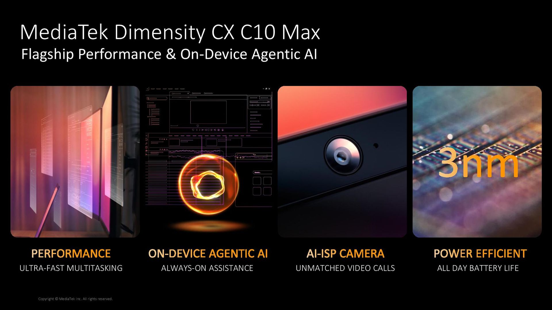
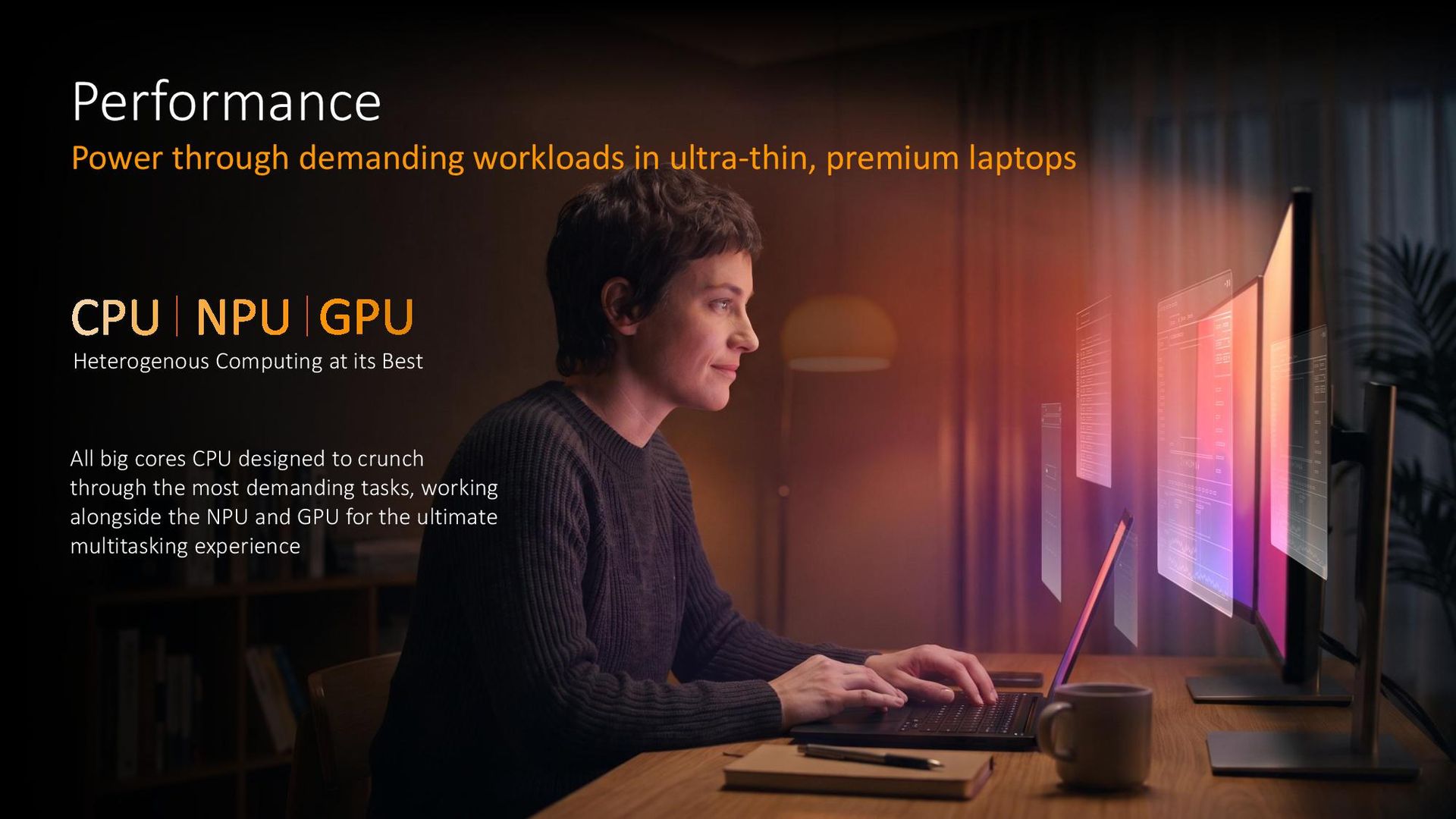
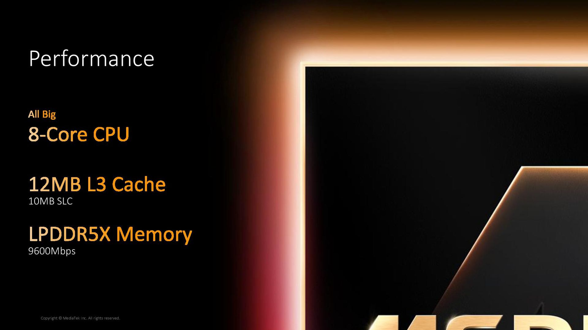
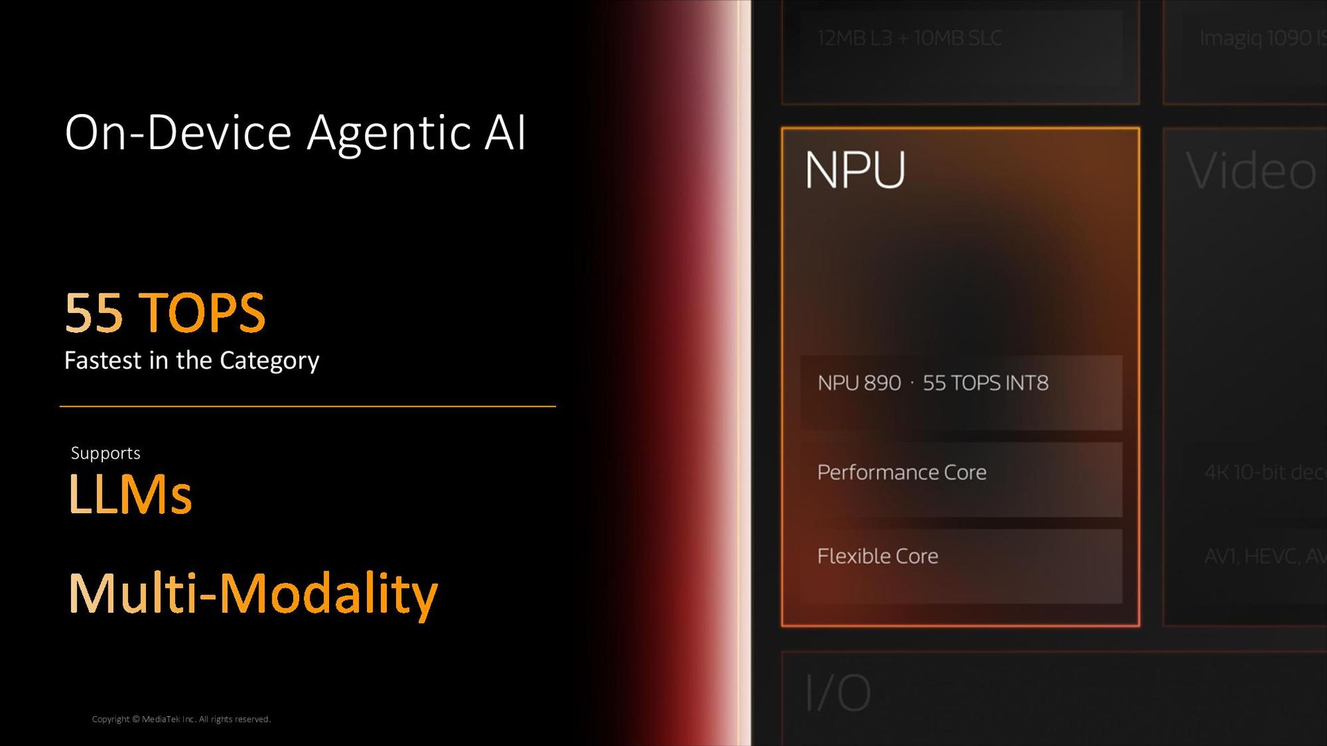
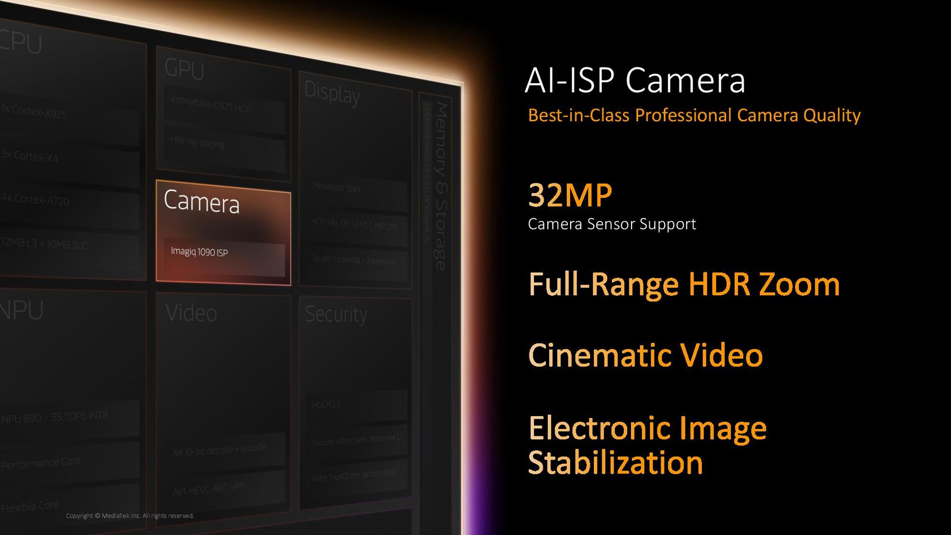
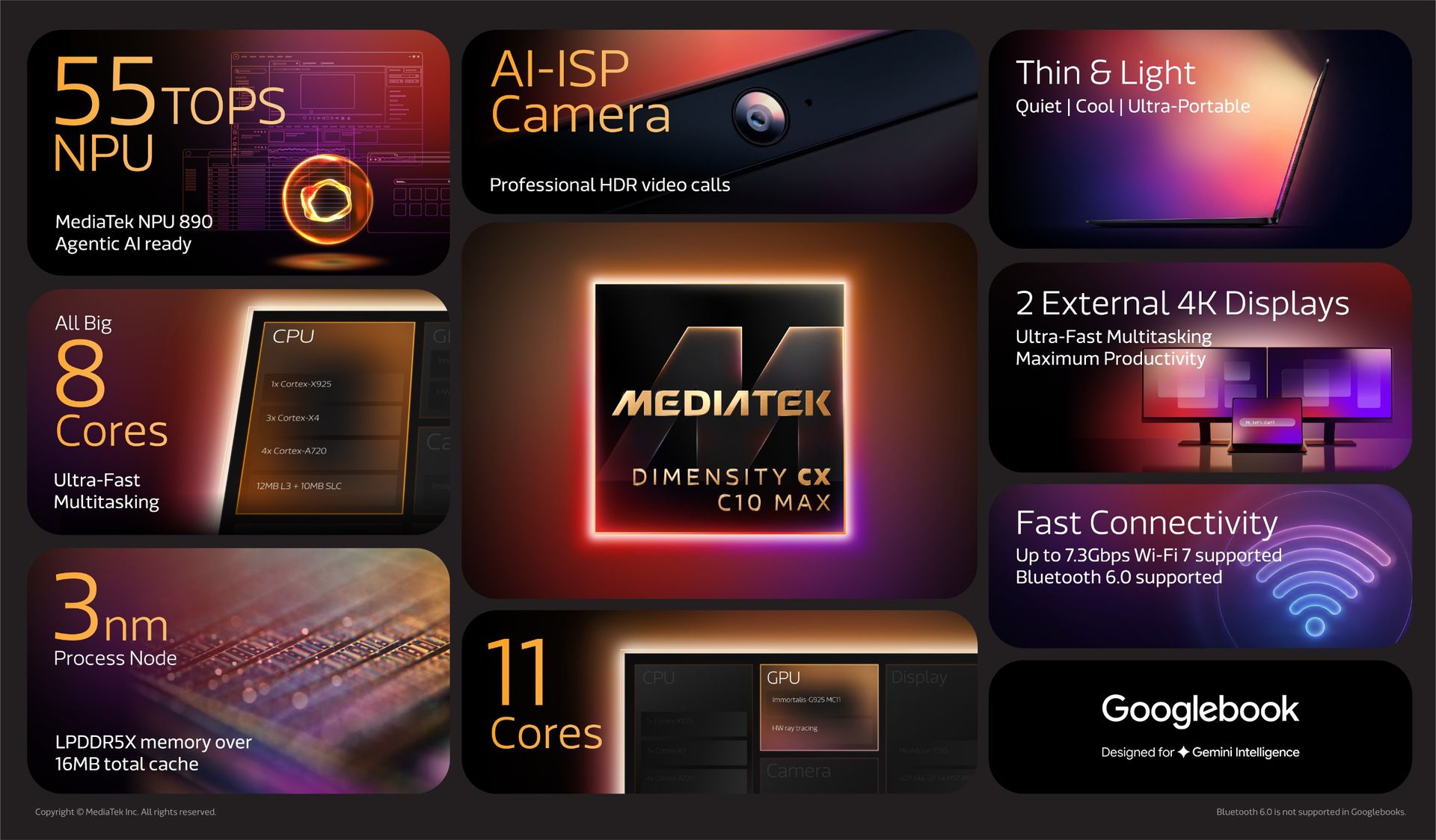
Google’s “brand-new category of flagship laptops,” called Googlebooks, will contain MediaTek’s next-gen Dimensity CX C10 Max processor, the first SoC to launch in the Dimensity CX lineup. It’s built on a 3nm node (TSMC N3) and uses an all-performance-core design, packing eight cores on the CPU and 11 cores on the GPU, along with MediaTek’s NPU 890, delivering up to 55 TOPS of AI performance, according to MediaTek. The new CX lineup will sit between MediaTek’s other offerings, between the RTX Spark in higher-end laptops and Chromebook with Kompanio chips.

MediaTek calls the C10 Max the “flagship of the lineup,” though we don’t have full specs on the chip, and not so much as a name for the other chips in the lineup. MediaTek is launching the CPU on the same day Googlebooks go on sale (September 21), and the company says it will power an upcoming Googlebook device. MediaTek hasn’t explicitly said that the chip is exclusive to Googlebook devices, though that seems likely given the company’s previous work with Google on Chromebooks.

The C10 Max is an “all big core” CPU, according to MediaTek, but not all eight cores are equal. MediaTek is using three different core types: one Cortex-X925 core, three Cortex-X4 cores, and four Cortex-A720 cores. The Cortex-X925 is the successor to the Cortex-X4, with higher clock speeds, a larger 10-wide decode, and larger L2 cache. The Cortex-A720 fits in a different range, though it was succeeded in 2024 by the Cortex-A725. This core split is identical to what MediaTek has used in its Dimensity 9400, 9400+, and 9500s mobile chips (though, presumably, the C10 Max will be afforded a larger power budget and higher boost clocks).

Perhaps more pressing, it’s identical to the core split in the Kompanio Ultra 910, MediaTek’s previous flagship in this category. The C10 Max features the same GPU and NPU, as well: the Arm Immortalis-G925 MC11 for the GPU and MediaTek NPU 890. The C10 Max also comes with the same 12MB of L3 and 10MB of system-level cache. The biggest difference, at least based on the specs MediaTek has shared, is memory speed. Both use LPDDR5X, but the C10 Max climbs up to 9,600MT/s from 8,533MT/s on the Kompanio Ultra 910.

C10 Max performance

(Image credit: MediaTek)

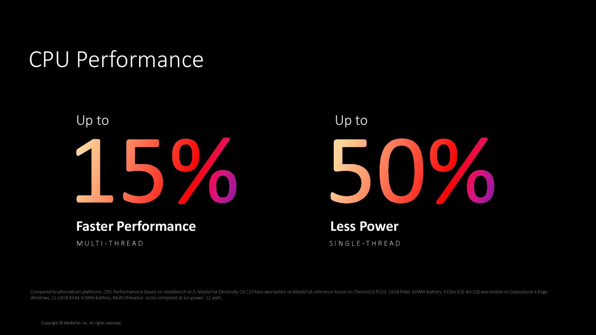
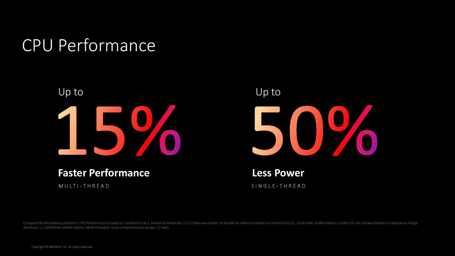
On performance, MediaTek has two rather vague claims, which you can see in the slide below. It claims the C10 Max has up to 15% faster multi-threaded performance and 50% lower power in single-threaded workloads, though without any mention of performance, compared to the Snapdragon X Elite X1E-84-100. That chip is the second from the top of Qualcomm’s last-gen X Elite stack, sporting 12 cores (8+4) and a 4.2 GHz boost clock. MediaTek says it used Geekbench 6.5 and ran the multi-threaded tests at iso-power, that being 12W (the X1E has a base TDP of 35W, and MediaTek didn’t clarify what power usage it was referencing).

Unfortunately, the performance numbers here aren’t worth much, at least not how they’re presented. Perhaps most notably, the test platforms were completely different, with MediaTek using a reference board running ChromeOS R133 for its chip and using a Galaxybook 4 Edge with Windows 11 from Samsung for Qualcomm’s chip. They’re only comparable on memory capacity (16GB) and battery (60Whr). MediaTek also didn’t share any actual numbers, leaving the claim about 50% lower single-threaded power usage dead in the water.

During a press Q&A, MediaTek VP of computing platforms PD Rajput said the C10 Max is competing with the X1 Elite, not Qualcomm’s newer X2 series. “In the category of devices we’re looking at, and the segment we’re on, it’s the X1E we’re competing with.” MediaTek didn’t share any performance numbers comparing the C10 Max to x86 CPUs from AMD or Intel.

Rajput also said that the Dimensity CX C10 Max won’t flow down to Chromebook or Chromebook Plus devices, saying MediaTek is “elevating our compute portfolio” with the C10 Max. We asked if the chip will come to Windows laptops as well, and the company said it’s only confirmed for Googlebooks at this time.

MediaTek battery life for C10 Max

(Image credit: MediaTek)

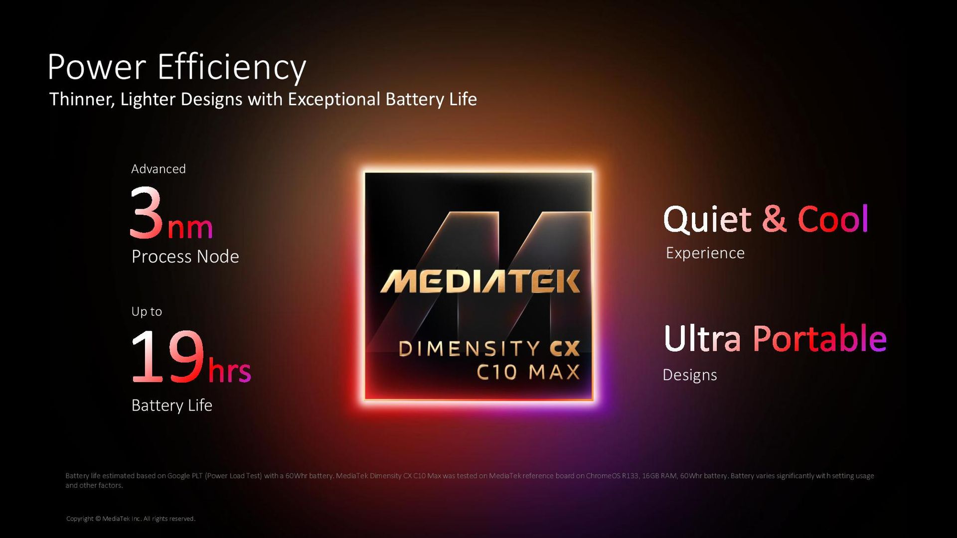
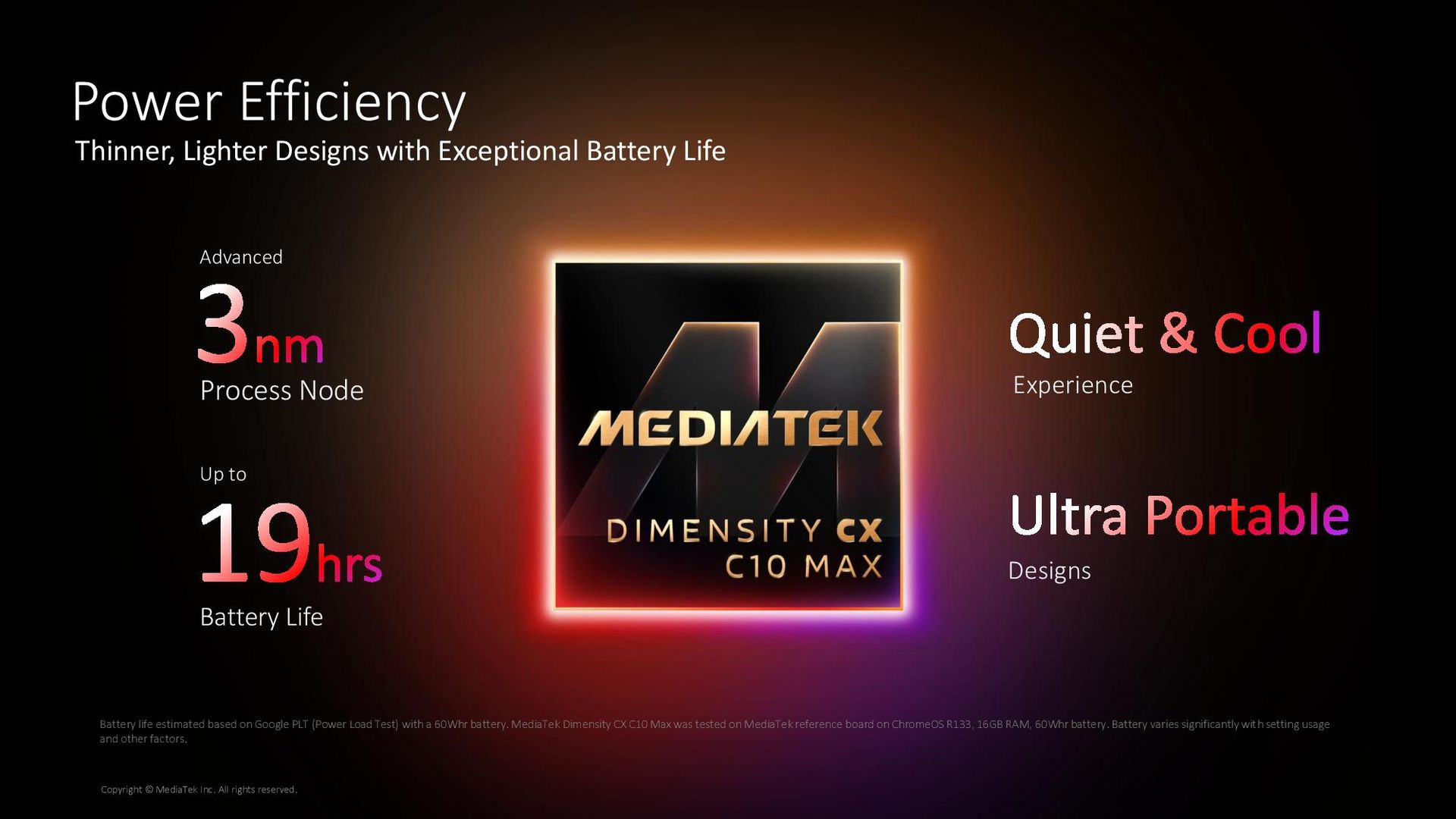
MediaTek says the C10 Max is capable of delivering up to 19 hours of battery life, which is certainly possible, though battery life is more of a system-level concern than a chip-level one. MediaTek arrived at that number testing a reference board with a 60Whr battery, so it's possibly the battery life could climb higher if the chip is paired with a larger battery.

Full MediaTek Dimensity CX C10 Max presentation

MediaTek C10 Max presentation
MediaTek
MediaTek C10 Max presentation
MediaTek
MediaTek C10 Max presentation
MediaTek
MediaTek C10 Max presentation
MediaTek
MediaTek C10 Max presentation
MediaTek
MediaTek C10 Max presentation
MediaTek
MediaTek C10 Max presentation
MediaTek
MediaTek C10 Max presentation
MediaTek
MediaTek C10 Max presentation
MediaTek
MediaTek C10 Max presentation
MediaTek
MediaTek C10 Max presentation
MediaTek
MediaTek C10 Max presentation
MediaTek
MediaTek C10 Max presentation
MediaTek
MediaTek C10 Max presentation
MediaTek
MediaTek C10 Max presentation
MediaTek
MediaTek C10 Max one sheet.
MediaTek

  •  

AMD targets Nvidia with first official benchmarks for EPYC 'Venice' CPUs — company claims 256-core chip is more than twice as fast as Nvidia Vera, 96-core model 20% faster per-core

Following the launch of AMD's EPYC 'Venice' CPUs in July, AMD extended the performance claims for its upcoming generation of server chips on Friday. The high-level claim hasn't changed. AMD still says a 96-core, high-frequency Venice chip is around 20% faster than Nvidia's 88-core Vera in SPEC CPU 2026's Integer Rate test. However, the company went into far greater detail about the benchmarks in a new white paper.

There are several configuration differences depending on the benchmark throughout AMD's white paper, and although we'll call out those differences here to the best of our ability, we don't have all of the details. For the Vera comparison, in particular, AMD is mixing data from different sources, and in some cases, using different major releases of the GNU Compiler Collection (GCC). That can have a substantial impact on performance, so keep your salt shaker handy.

Venice benchmarks

(Image credit: AMD)

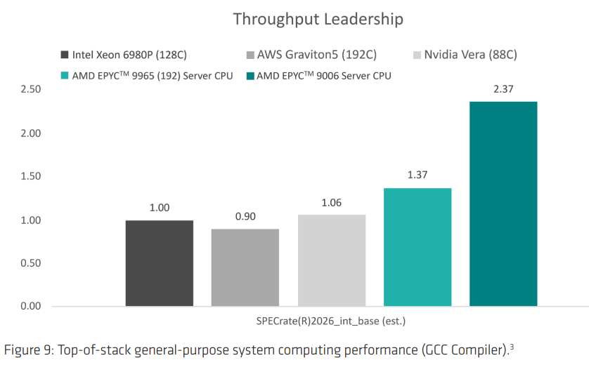
First up are results in SPEC CPU 2026 with the intrate test, looking at total throughput. These are older numbers, gathered in July with GCC 15.2. The intrate test runs multiple copies of an application on the same CPU, and the SOP is to run one copy per thread. Presumably, that's what AMD did here, but the white paper doesn't clarify, even in the footnotes.

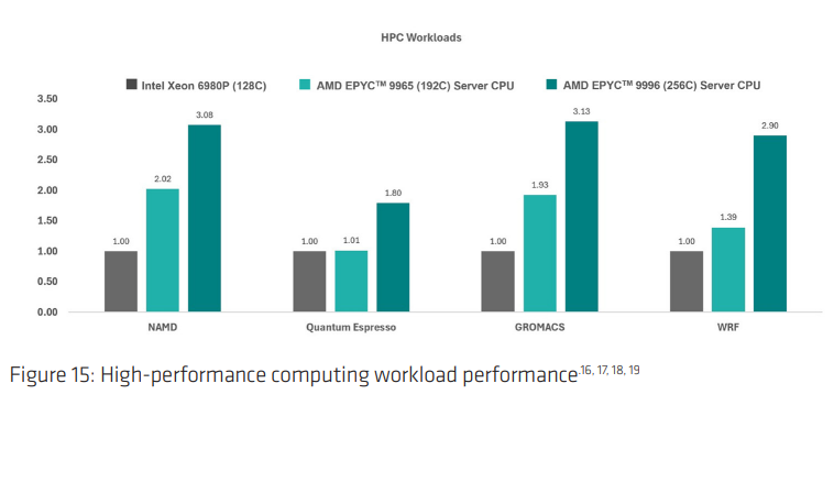
The 256-core 9996 is 2.37x faster than the Intel Xeon 6980P and 2.24x faster than Vera according to the slide. The white paper clarifies the mystery 9006 CPU is the 256-core flagship. Perhaps most impressive is AMD's gen-on-gen comparison. According to these results, the 9996 is around 78% faster than last-gen's 192-core EPYC 9965.

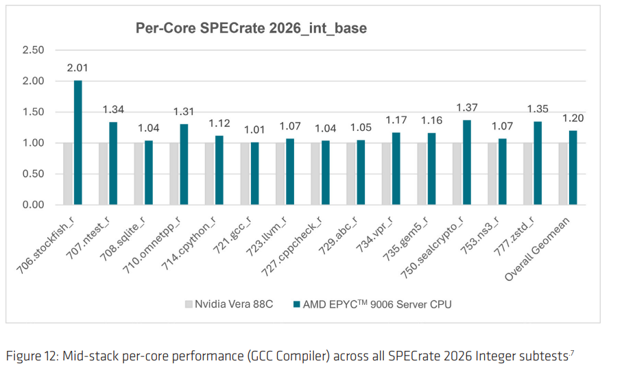
Although the high-level results bring in data from Intel and AWS, much of the white paper focused squarely on the comparison between Venice and Vera. AMD broke down the individual subtests of SPEC CPU 2026 intrate in the white paper, which you can see below.

Venice benchmarks

(Image credit: AMD)

The comparison looks good for AMD, naturally, though there are a few wrinkles in the configuration. AMD is testing a down-cored EPYC 9996, dropping from 256 cores to 96 cores. It made no mention of power budget, but when AMD originally shared SPEC numbers, the 96-core model had access to the same 600W as the 256-core model — AMD's 96-core, high-frequency Venice SKU tops out at 500W. More consequential is the compiler, however. AMD is using GCC 16.1 and comparing the results to the ones Nvidia shared in its Vera white paper. Nvidia used GCC 15.2.

Michael Larabel over at Phoronix has a nice write-up about the difference between GCC 15 and 16, but the short story is that there are performance differences, not always for the better. GCC 16 takes longer to compile due to better optimizations, hence the lower scores on the GCC and LLVM compilations above. However, that leads to faster binaries. By how much depends on the flags, software, and a whole host of other factors. Regardless, it's not best practice to compare benchmarks using two different compiler versions. It makes sense that AMD used GCC 16.1 — it includes support for Zen 6 — but ideally Vera would also be on GCC 16.1.

Venice benchmarks

(Image credit: AMD)

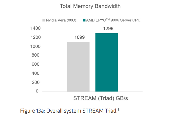
Speaking of Phoronix, AMD pulled some data for the publication's initial, controlled testing of Vera. Above, you can see the Stream, an industry-standard benchmark for measuring memory bandwidth. Again, AMD is using a down-cored 9996 from 256 cores to 96, and offering it a 600W power budget. Still, this is an impressive showing, as Vera absolutely clobbered the competition in the publication’s original Stream results. Here, AMD is ahead by about 18%, with per-core performance about 8% ahead.

Venice benchmarks

(Image credit: AMD)

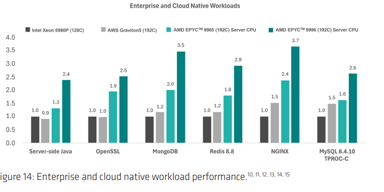
Breaking out of Vera, AMD also showed performance in cloud workloads, including database, Java, and cryptography. Once again, the gen-on-gen comparison stands out, as AMD was already leading in these workloads with its last-gen chips. AMD ran these tests itself, rather than relying on third-party data, though the Graviton5 results came from an AWS cloud instance.

Venice benchmarks.

(Image credit: AMD)

Similarly, in HPC workloads, AMD furthers its lead over Intel's flagship Granite Rapids-AP offering. Intel's next-gen data center CPUs, codenamed Diamond Rapids, are set to be released next year.

Venice benchmarks

(Image credit: AMD)

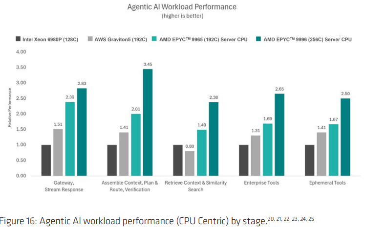
Finally, we have "agentic AI workload performance," which uses actual benchmarks for comparison, despite what the names in the chart above suggest. From left to right, AMD used NGINX, TPCx-AI kit, FAISS, TPC-H and TPC-C, and a replay of a multi-persona agent. For TPC-H and TPC-C, AMD says it derived workloads from those benchmarks, so the results here aren't comparable to published results.

Although looking at benchmark results is always interesting, it doesn't say much in the context of a server deployment, at least at the scale that AMD is targeting. Peak performance is only one of the major factors that go into server deployments, after all, and even then, performance can vary wildly depending on what software you're running and how it's built.

Still, Venice looks impressive, perhaps more so in the gen-on-gen comparison than any competitive comparison. Hopefully that bodes well for AMD's future Zen 6 rollout on consumer desktops, but we'll have to wait until Team Red has more to share before drawing any conclusions on that front.

  •  

Details about Intel's next-gen Nova Lake CPUs keep leaking — an attempt to establish a timeline based on what we know so far

Intel's Nova Lake CPUs are no stranger to leaks. We've been talking about the processors for close to two years now, with rumors swirling about bLLC and a 52-core flagship for well over a year. However, this week (and this month more broadly), we've seen leaks hit a fever pitch, suggesting that Intel is finally gearing up to release a generation of processors that's been the zeitgeist for over 24 months.

Intel hasn't shied away from discussing Nova Lake, with Intel's enthusiast channel VP Robert Hallock telling Tom's Hardware Premium that it's one of the most important launches for the company ever. At the beginning of the year, Intel CEO Lip-Bu Tan said that Nova Lake would launch in the second half of 2026, and despite expected hubbub about delays/cancellations, that's the North Star Intel itself has set. So, that's also going to be our North Star here.

There are three stories that have come out over the past week and a half. First, a screenshot of some high-level details about Nova Lake surfaced online, showing the launch schedule and platform details. The slide in question is almost certainly from one of Intel's partners and not Intel itself.

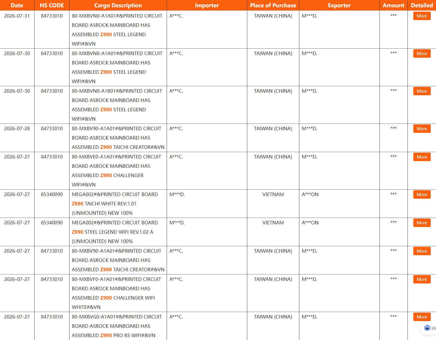
Just in the past few days, we've also seen a barrage of Z990 motherboards from ASRock surface in the NBD shipping database, as well as some entries in the SiSoftware database for a next-gen HP EliteBook X sporting an unknown Intel processor.

The NBD database showing Z990 shipments.

(Image credit: Tom's Hardware)

An increase in the number of leaks/rumors, especially those that are more than a known leaker writing up a post on X, usually points to an imminent launch. We've heard about Nova Lake for over two years, yes, but now we're seeing more concrete details. In addition to the shipping manifest, snapped slide, and SiSoftware results, we also saw two Z990 motherboards ourselves at Computex earlier this year, with a third rumored. We will not predict the Nova Lake release date here. However, the launch is coming soon. That much we're confident in.

Intel's typical release cycle for desktop CPUs

In order to establish a timeline, we first need to look back. We could go back far, but we're cutting the timeline short here at Alder Lake. That was when Intel finally moved off 14nm, following generation after generation of either an underwhelming launch or a delayed one, and it's most relevant to what Intel is doing today.

Intel desktop CPU release cadence

Generation

Announcement Date

Release Date

Alder Lake (12th-Gen)

October 27, 2021

November 4, 2021

Raptor Lake (13th-Gen)

September 27, 2022

October 20, 2022

Raptor Lake Refresh (14th-Gen)

October 16, 2023

October 17, 2023

Arrow Lake (15th-Gen)

October 10, 2024

October 24, 2024

Arrow Lake Refresh (15th-Gen Plus)

March 11, 2026

March 26, 2026

The timeline above is fairly straightforward. Intel has, short of 2025, launched a new generation of desktop processors in the fall every year for the past five years. This annual cadence was even more intense previously; 7th-Gen and 8th-Gen CPUs were both released in 2017, and 9th-Gen in 2018. Then, Intel took a year off and followed up with 10th-Gen in 2020 and 11th-Gen in early 2021. Keep in mind that we're talking about desktop CPU launches with a new microarchitecture here. Obviously, Intel has released a ton of other products in between the gaps.

The interesting bit about the timeline is actually the end with Arrow Lake Refresh. When we spoke to Robert Hallock earlier this year, he told us that a team that was "pretty much completely different" worked on Arrow Lake Refresh compared to Arrow Lake. That might explain the strangely large gap between Arrow Lake and Arrow Lake Refresh. Even looking at the Arrow Lake and Arrow Lake Refresh stacks side-by-side, it's obvious that a different mentality went into how they were positioned in the market. That team is in in-place now, and Hallock told us the team is "moving faster than we ever have in product, in release cadence."

Don't take Hallock's comments about Intel moving faster than ever at face value — he was probably being at least a little hyperbolic — but the sentiment is clear. Following the poor reception of Arrow Lake, Intel reorganized and set a new roadmap in motion that extends out to 2030, and now, that roadmap is being executed, starting earlier this year with Arrow Lake Refresh. That sets up Arrow Lake Refresh similar to 11th-Gen Rocket Lake, serving as somewhat of a stopgap before the next generation properly arrives (that is, thankfully, where the comparisons between Arrow Lake Refresh and Rocket Lake end).

Back to Nova Lake. Earlier this year at Computex, we saw two Z990 motherboards, one of which we confirmed was not a finalized unit. The complete development process takes generally four to six months for a motherboard, and you can add another two months or so on top of that for channel sales, as pallets of PCBs are loaded onto ships and swim across the Pacific Ocean. That was in June.

The shipping manifest that surfaced this week showed shipments in July for ASRock. Critically, it also shows shipments from two different sources: Taiwan and Vietnam. Given what we saw at Computex and the two different sources for ASRock, we're firmly past the early prototype and engineering validation stage of motherboard design. Assuming everything goes according to plan, that means Z990 motherboards should be ready to go on store shelves by no later than October or November.

Keep in mind that does not mean Nova Lake will launch in October or November, just that motherboards will most likely be ready by then. This aligns with what motherboard vendors told us earlier this year, with some brands pointing to Q3 but most to Q4 for a Z990 rollout.

Parsing the details about Nova Lake so far

Currently, there are two camps when it comes to when Nova Lake will release. Some say it'll arrive this year, likely in Q4, while others say CES 2027 in January of next year. As we wrote earlier in the article, we will not predict the Nova Lake release date. However, we will side with one of the camps here as more likely based on what we've seen so far.

Given everything we've seen, a late 2026 launch is more likely. The strongest evidence of that is the comment from Tan earlier this year, where the executive said Nova Lake is "coming at the end of 2026." The critical context is that Tan made that comment as part of his prepared remarks, preceding the actual financials that you hear in an earnings call. An earnings call is not a keynote, and making material promises you knowingly can't keep can land you in hot water.

Executives massage the truth all the time during earnings calls — that's half the reason there are prepared remarks ahead of the financials. However, that key detail about an end of 2026 launch isn't massaging the truth. It's a concrete claim devoid of weasel words and qualifiers. In addition, Intel's fiscal year aligns with a calendar year; when Tan said end of 2026, he meant end of 2026, regardless of fiscal or calendar year.

It's possible that something changed between now and January when that call took place. However, the timeline still lines up given the various motherboards that showed up between June and July of this year. At this point, Intel can slide the actual release date around by a bit, but not by months. Retailers aren't going to sit on pallets of motherboards with no home indefinitely.

https://t.co/iDacFgR89aSeptember 3, 2026

The one wrinkle in this is the leaked slide you can see above, which claims Nova Lake will enter mass production in Q4, with a launch in Q1 2027. There are reasons to be skeptical of this slide, however. For starters, the slide doesn't say anything that hasn't been heavily rumored for months (sometimes even years) at this point: 52-core flagship, up to 288MB of bLLC, LGA 1954 socket, and multi-generation socket support. The strange bit is a mention of Hammer Lake at the bottom of the slide.

We've heard very little about Hammer Lake, and nothing that's passed muster for us to cover on Tom's Hardware. Even among the rumors, the launch has been pinned somewhere in the 2029/2030 range, if the lineup is even real to begin with. Regardless, Hammer Lake isn't what we'd expect to see next to Razor Lake — the generation rumored to follow Nova — and certainly not what we'd expect to see under a "Q4 2027+" badge.

That doesn't mean the slide is fake; it doesn't appear to be fake. There's some very critical context missing from it, though. It's a Chinese source, but did it come from an OEM? A distributor? A retailer? The validity of the slide changes dramatically depending on that. Further, we're only seeing maybe half of a single slide here. There's too much context missing to take this single slide and run with it as concrete truth.

At the very least, it fares poorly against prepared comments made by Intel's CEO, motherboards we've seen (and held) ourselves, and have circulated through photos online, and strong indications from Intel's motherboard partners that they'll be ready for a launch in Q4. Add on top of that the fact that Intel took 2025 completely off for new desktop launches (and its usual cadence of launching in the fall), and a Q4 rollout of Nova Lake looks far more likely.

Likely isn't the same as confirmed. We're still awaiting details on Nova Lake from Intel proper, and hopefully those will arrive soon. Given the anticipation Intel has already built around Nova Lake without a single performance claim or spec shared, we'll have a lot to talk about.

  •  

Balatro fan claims they trained Google fruit fly brain simulation to beat the game — reinforcement learning currently has the model at 20% success rate

Less than two weeks after Google released a mapping of the complete brain and central nervous system of an adult male fruit fly, we've seen enthusiasts put the structure to work everywhere from turning a fruit fly into a day trader to teaching it parallel parking. Now, one Balatro fan says they trained the structure with an algorithm to play the game, with the win rate currently sitting at a cozy 20%.

The famous Fruit Fly has beaten Balatro
 from r/balatro

The player shared a sped-up video of the model apparently playing the game. Based on the video, the player chose the lowest difficulty (White Stake) and the default Red Deck. We've already seen OpenAI's GPT-6 'Astra' model beating the game with the Black Deck on Gold Stack difficulty, which is generally considered the hardest combination in the game.

ActualAerie1011, the Reddit user who shared the video, says they trained the model using a trainer algorithm they developed to discover useful Balatro seeds. Like other roguelike games, Balatro is randomized, so algorithms like this can discover seeds that are unique and can potentially lead to very high scores (including the game's scoring limit). In order to train the brain, both the brain apparatus (a connectome alongside the actual model) and the algorithm play a seed. Then, the results are compared, and the model on the brain is rewarded or punished based on its choices.

Currently, the user says that the brain has a 20% success rate on a random seed, presumably at that same White Stack/Red Deck difficulty. The user says the model doesn't know anything about the seed outside of what's immediately visible on-screen, and that training is ongoing. "The fruit fly will return, strong and smarter," they wrote in a comment on their original post.

It's an impressive feat, though some commenters have cast doubt on the project. The player didn't share many details about how they trained the model outside of what's above, nor any repo for the project or references to other open-source projects they used. This isn't uncharted territory for Balatro; projects like BalatroBot and BalatroLLM have been available for about a year.

We've reached out to ActualAerie1011 to see if they're able to provide more details on how they trained the model, and we'll update this story when we hear back.

Although Balatro seems straightforward enough, it's surprisingly difficult to train a model to play the game, especially at higher difficulties. The core rules of playing and scoring poker hands aren't difficult. However, the complex interactions between jokers (the perks that help you achieve higher scores), how they're ordered and scored, and specific stipulations like boss abilities and temporary/permanent jokers make consistency a high bar to clear, even for human players, much less an AI model.

  •  

Intel reportedly cans 12Xe option for Nova Lake-S desktop — gaming APU design said to resurface with Razor Lake

Intel won't launch a Nova Lake-S SKU with 12 Xe3P graphics cores, according to tipster Jaykihn, who originally flagged a beefed-up APU design with the Nova Lake architecture. The original SKU was said to come with 4 P-cores, 8 E-cores, and 4 LPE-cores, along with the 12 Xe3P cores, presumably offering an inexpensive onramp to a gaming desktop without a discrete GPU. Now, the leaker says that design is cancelled, and Intel intends to pick it back up with Razor Lake, the generation that will follow Nova Lake.

Nova Lake -S 12Xe has been changed to Razor Lake -S 12XeSeptember 14, 2026

Originally, Intel's 12 Xe3P Nova Lake SKU was said to require 65W of dedicated power to drive the iGPU, necessitating the use of two VCCGT phases on the motherboard for integrated graphics. Intel's Arc B390 GPU, which is the 12 Xe3-core model available in Panther Lake and Arc G-series processors, has a thermal design that can sustain up to 80W. However, it's currently being used in Panther Lake machines and handhelds like MSI Claw 8 EX AI+ that have lower power targets.

The Xe3P architecture is slotted for use in Intel's Crescent Island AI accelerator, but it hasn't been announced for any other products yet. Xe3P supports a wide deployment of Xe cores (up to 32), a deeper XMX engine with support for low-precision data types like FP8 and FP4, an increased 512KB L1 cache per Xe core, and a new unified L2 cache (32MB on Crescent Island).

Even by desktop APU standards, an 80W iGPU is a beefy accelerator to have on the same package. In addition, Intel's Nova Lake stack is said to extend up to a 175W TDP with the rumored top-end 52-core SKU, meaning the full 12 Xe3P iGPU would likely only be possible lower down the stack (and maybe only in the 4 + 8 + 4 + 12 Xe design originally suggested).

Earlier in the year, rumors suggested Intel was working on a mobile APU to counter AMD's Strix/Gorgon Halo products, featuring a large pool of unified memory and a large iGPU, dubbed Nova Lake AX. Now, the rumor mill suggests Intel will recycle the Nova Lake CPU cores for Razor Lake AX on mobile while pushing a larger iGPU.

Nova Lake-S rumored specifications

SKU*

Core Config (P+E+LPE)*

bLLC*

TDP (Unlocked/Locked)*

52 Cores (dual-tile)

(8+16)+(8+16)+4

288MB

175W

44 Cores (dual-tile)

(8+12)+(8+12)+4

264MB

175W

28 Cores

8+16+4

144MB

125W

28 Cores

8+16+4

-

125W / 65W

24 Cores

8+12+4

132MB

125W

24 Cores

8+12+4

-

125W / 65W

22 Cores

6+12+4

108MB

125W / 65W

22 Cores

6+12+4

-

125W / 65W

16 Cores

4+8+4

-

65W / 35W

12 Cores

4+4+4

-

65W / 35W

8 Cores

4+0+4

-

65W / 35W

6 Cores

2+0+4

-

65W / 35W

*Specs rumored, unconfirmed by Intel

Intel has told us that Nova Lake is one of the most important desktop CPU launches for the company ever, following on the heels of the mediocre Arrow Lake rollout. Perhaps the biggest addition to the lineup is rumored to be bLLC, or big last-level cache, which is said to show up on select SKUs to counter AMD's X3D assault among the best CPUs for gaming. The company has yet to confirm that bLLC is even possible with its current packaging capabilities, though enthusiast channel VP Robert Hallock hinted to Tom's Hardware that Intel has plans to address X3D in the next generation.

The main stack is rumored to climb up to 28 cores, with two additional dual-tile SKUs that can go as high as 52 cores. The dual-tile models look like a bid for HEDT, perhaps competing with AMD's Threadripper CPUs, though it's not clear how Intel will position its dual-tile models yet.

Earlier this month, a leaked slide gave us a glimpse into Intel's launch plans for Nova Lake. The slide suggested Intel will announce the main stack (up to 28 cores) in Q4 of this year, with the chips arriving in Q1 2027. Intel will apparently follow up later in the year with the 52-core model. This aligns with what we've heard from our sources about Intel's Nova Lake rollout.

Alongside Nova Lake, Intel will introduce the new LGA1954 socket, along with the flagship Z990 chipset. We've already seen multiple Z990 motherboards in the flesh, suggesting Intel is preparing for a Nova Lake release in short order.

  •  

Nvidia's RTX 5090 vanishes from online retail in the US — third-party sellers now demand as much as $9,500 for Nvidia's fastest GPU

Nvidia's fastest gaming graphics card, the RTX 5090, has been on a tear of price increases over the past several weeks. However, over the past week, the available inventory has dwindled. Now, you can only find the RTX 5090 from third-party sellers at online retailers like Newegg and Amazon, commanding anywhere from $6,500 to $9,500 (or even higher) for Team Green's best GPU.

At Newegg, the cheapest RTX 5090 is the MSI Ventus 3X that's available from Slava Computers (a relatively new seller with 239 ratings and a 2.8 out of 5 rating at the time of writing) for $6,449. On Amazon, you can get the Asus TUF Gaming OC for $6,395 from Joes Tech Shop, a seller with an 81% positive rating. However, among the most recent reviews are a string of one-star reviews about orders never being fulfilled. The cost goes much higher, as well. The first result for "RTX 5090" on Newegg, for example, surfaces the MSI Ventus 3X OC for $8,699.

In June, the median price for an RTX 5090 was $4,299. At the beginning of September, we logged the lowest online price at $5,199 in our GPU price tracker. Now, in less than two weeks, the available stock has completely disappeared online, and the options available from third-party sellers have ballooned in price once again.

Naturally, we don't recommend buying from one of these third-party sellers. The RTX 5090 is selling at a vastly inflated price, but more importantly, we've seen no shortage of scams around high-ticket items like the RTX 5090. In January, 42 Amazon customers were duped into a scam involving a $999 RTX 5090, instead receiving a fanny pack in place of the GPU. Earlier this month, an online seller scammed two buyers with the RTX 5090, selling phantom graphics cards with the core and memory removed on the secondhand market for prices near MSRP.

The one exception to RTX 5090 inventory is Micro Center, which still has cards available around the average selling price. At a local Micro Center we checked, the cheapest in-stock option was $4,299. Micro Center has exclusively sold graphics cards in-person for several years, insulating it from online buyouts like what appears to be going on right now.

As usual, the reason why there's so much demand for the RTX 5090 is fairly obvious: AI. The RTX 5090 holds the GB202 GPU and 32GB of GDDR7 memory. For context, Nvidia's RTX Pro 5000 48GB comes with the same GPU with a third fewer shader units enabled, and lower memory bandwidth compared to the RTX 5090, and sells for between $7,000 and $9,000. In that context, the RTX 5090 starts to look attractive for building an AI server, even at $5,000 (or more) apiece.

At the same time, the RTX 5090 remains the fastest gaming graphics card on the market according to the testing in our GPU benchmark hierarchy. That's even more true now with Nvidia's launch of DLSS 5 Neural Rendering, which the RTX 5090 can fully capitalize on (though, thankfully, we've found playable performance on lower-end cards in our extensive DLSS 5 testing).

We've reached out to Nvidia for comment on whether it has any plans to stabilize inventory. We'll update this story when we hear back.

  •  

Intel-backed auto-overclocking tool Hypertune optimizes individual systems, not test profiles — tool claims FPS improvement of up to 60% on Intel-based systems

Following an early access period that included over 60,000 participants, auto-overclocking tool Hypertune has released its Gaming Performance Engineering platform, which is built on top of Intel's Extreme Tuning Utility (XTU) SDK and developed in partnership with Intel. The company claims the utility can boost frame rates by up to 60%, though you shouldn't expect that as the norm. The tool includes automated CPU and GPU overclocking, as well as customizable Windows features, network optimization, and game-specific optimizations.

Hypertune partnered with Intel to build the tool, which the company says "evaluates each supported system individually" before optimizing rather than relying on generalized profiles. In its press release, Hypertune says it collaborated with famed overclocker SkatterBencher (Pieter Plaisier) to refine the software. We've reached out to Plaisier to confirm their involvement.

Automated tuning programs usually don't work as well as advertised, and we haven't had the chance to test Hypertune ourselves yet. Especially on more recent hardware, expect performance gains to be minor. Hypertune shared some of its internal benchmarks to back up the claim, showcasing the actual test systems it used, the numbers it gathered, and what each step of Hypertune contributed to the performance increase.

Hypertune performance.

(Image credit: Hypertune)

Hypertune tested two systems: one with a Core Ultra 9 285K and an RTX 5090, and another with a Core i7-14700K and an RTX 3080. For the 285K system, the team saw an 18.9% improvement in Homeworld 3 and a 28.2% improvement in Tomb Raider. For the 14700K system, the boost was up to 9.8% in Rainbow Six Siege and 4.3% in Marvel Rivals.

Notably, these results are with Hypertune's Game Hub disabled. Game Hub automatically applies a graphics settings profile to select games, leading to massive increases in performance. Naturally, tweaking your own graphics settings in the same way leads to the same result.

Hypertune performance in Homeworld 3.

(Image credit: Hypertune)

In Homeworld 3, you can see how each step in the process impacted performance, with CPU tunning contributing the single biggest increase in performance. As shown by Marvel Rivals in Hypertune's data, some games will see little to no benefit from Hypertune, though select titles with certain hardware may see a significant performance increase. In this case, the Core Ultra 9 285K has plenty of room for overclocking, and Homeworld 3 is particularly sensitive to the CPU, so the uplift makes sense.

Hypertune performance in Rainbow Six Siege.

(Image credit: Hypertune)

Elsewhere, the gains aren't as pronounced. In Rainbow Six Siege, you can see that Hypertune contributed about a 9.8% jump in performance, though the vast majority of the improvement comes through Game Hub, where Hypertune changes in-game settings.

In a press release, Hypertune founder Austin Copeland wrote that the team was "not trying to build a tool for overclockers," suggesting it's aimed toward users who may not know about specific settings (i.e., the Balanced power plan on dual-CCD X3D CPUs, or HAGS for DLSS Frame Generation). Copeland was previously a coach for eSports organization TSM, coaching Valorant teams under the name "Apex."

Hypertune at Intel overclocking lab.

(Image credit: Hypertune)

Hypertune works through Intel's XTU SDK, and the company says its optimizations are non-destructive and fully reversible. The software is mainly targeted toward competitive titles (naturally, given Copeland's background), but it can apply optimizations globally across the system. Hypertune says it's safe to use with anti-cheat software, including Riot Vanguard, Easy Anti-Cheat, and BattlEye.

Although there are plenty of free tools that claim to optimize your system, Hypertune isn't among them. It's a subscription service, available for either $9.99 per month or $59.99 per year. In addition to software, Hypertune offers its "expert tuning" service for $80, where a technician will remote into your machine and manually tune it. On the subscription front, Hypertune offers a 7-day free trial.

Hypertune looks like one of the more robust automated overclocking tools we've seen, but it's worth highlighting that, in most cases, these tools don't do anything you can't accomplish yourself. If you're looking for a starting point, make sure to read our guides on how to overclock your graphics card and how to overclock your CPU.

  •  

Intel reportedly set to hike CPU prices by 10% ahead of 'major annual product' launch in March 2027 — report says AMD will follow up between June and July

Intel is reportedly set to hike CPU prices by 10%, according to a new Digitimes report. Citing supply chain sources, the outlet says the increase follows two others, one in the first quarter of 2026 and another in July, among some server and client CPUs. Notably, the sources didn't say which products the price increase applies to, though presumably, the increases would come through Intel's mobile and server businesses before desktop client. Citing industry sources, DigiTimes also reports that Intel is set to launch "major annual products" in March 2027, with AMD following up with launches of its own between June and July.

The increases come on the back of Intel seeking higher gross margins for its products as the PC market shrinks. This is a story we've heard directly from Intel in the past. In its most recent earnings call in July, Intel chief financial officer David Zinsner attributed a 13% YoY increase in Intel's client revenue to higher average selling price, not a higher volume of sales.

Although the Digitimes report doesn't clarify which products will see a price increase, server and mobile seem like the most likely candidates. Intel's most recent Panther Lake calls for high-speed LPDDR5X-7467 memory as a minimum, and last-gen Lunar Lake CPUs have on-package memory. Naturally, higher memory prices put more pressure on fully built systems like laptops more so than socketed, standalone desktop processors.

On the server end, there's been an unprecedented increase in demand for server CPUs on the back of agentic AI workloads. That demand led to several consecutive records for Intel's share price, even without any major product announcements. Earlier in the year, Wall Street estimated the server CPU market would rise to around $120 billion by 2030 (currently around $30 billion). Now, those projections go up to as high as $220 billion.

According to the report, Intel is set to launch a major new annual product in March 2027, followed by AMD between June and July. Last week, a leaked Intel roadmap showed the company's next-gen Nova Lake desktop CPUs entering mass production in Q4 2026 with a release in Q1 2027, lining up with DigiTimes' report.

Although the timelines line up, the rumor mill has suggested an early Q1 launch for Nova Lake. It's worth noting that the DigiTimes report doesn't make mention of which product Intel will launch in March. This year, for instance, Intel launched its Xeon 600 CPUs for HEDT in March.

Perhaps more interesting is the AMD timeline. We already know of one major AMD product launch in the second half of 2027, which is Venice-X. Those are Zen 6 server CPUs with AMD's 3D V-Cache, packing up to 1,152 MB of L3 cache on the chip. Otherwise, that timeframe seems to point to AMD's next-gen desktop CPUs with the Zen 6 architecture, codenamed Olympic Ridge.

AMD launched its Venice server CPUs earlier this year, the first sporting the Zen 6 architecture. We haven't heard anything official about Zen 6 in the desktop yet. That's strange given AMD's last several releases. There was about a two-year gap between Zen 3 and Zen 4, as well as Zen 4 and Zen 5, on desktop. We've just crossed the two-year mark for Zen 5, so assuming AMD keeps a similar launch cadence, we'd expect to hear something sooner than June or July or next year.

That same explosive demand in server CPUs could have changed AMD's launch plans, however. Given that we haven't heard anything official about Olympic Ridge at this point, a launch in June or July isn't out of the question.

  •  

Arm debuts next-gen semi-custom Neoverse CSS N4 ‘Falcon' platform — compute subsystem packs up to 128 cores per die on TSMC N3P

Arm is bringing its next-gen Neoverse CSS N4 platforms to the cloud, sporting up to 128 cores per die, built on TSMC’s N3P process. Arm’s Compute Subsystem, or CSS, is a semi-custom program that allows customers to design a chip based on Arm’s IP, configuring components like core count, cache size, I/O, and connectivity to fit their specific needs. It’s the same platform we’ve seen at work everywhere from CPUs at Azure and Google Cloud to DPUs at Nvidia and Intel.

Arm says Neoverse CSS N4 supports between eight and 128 Neoverse N4 cores, running up to 3.8 GHz. Presumably, the clocks drop as the core count rises; Arm didn’t clarify the maximum clocks for each possible configuration. At a system level, Neoverse CSS N4 can scale beyond 128 cores, with support for multi-chiplet and multi-socket designs, and with support for UCIe through chip-to-chip interconnects, as well as “partner-specific PNYs.”

The platform supports either DDR5 or LPDDR6, and features up to 256 MB of L3 cache per die. For local cache, Arm includes up to 2 MB of L2 per core, as well as 64 KB of L1 instruction cache and 64 KB of L1 data cache per core. For I/O, Arm supports up to 128 lanes of PCIe 7/6 and CXL 4.0.

It’s a significant upgrade over the Neoverse CSS N2 platform, which topped out at just 64 cores, 1 MB of L2 cache per core, and 64 MB of L3 cache, paired with either DDR5 or LPDDR5 and 64 PCIe 5.0/CXL lanes.

Arm Neoverse CSS N4 platform.

(Image credit: Arm)

With 128 cores running at 3GHz and 2MB of L2 cache per core, Arm says Neoverse CSS N4 delivers twice the socket performance of Neoverse N3, 1.25x performance per watt, and 1.75x the memory bandwidth.

Arm’s N-series cores are optimized for performance per watt, while its V-series cores are targeting maximum performance. For instance, Arm used the Neoverse CSS V3 building blocks for its own AGI CPU, and Nvidia used Neoverse V2 for its last-gen Grace CPU (the Vera CPU uses a custom core). AWS has also used Neoverse V-series cores for its own Graviton chips, as does Google Cloud for Axion.

N-series cores aren’t usually deployed in high-performance CPUs. Rather, they fit into less-performant accelerators, such as Intel’s IPU Adapter E2100, which is built on Neoverse N1 cores. We’ve also seen it deployed in less-demanding, cloud-based workloads, such as through Microsoft’s Azure Cobalt 100, which is built on Neoverse N2. Cobalt 200 moved onto Neoverse V3.

We don’t know much about the Neoverse N4 cores, codenamed Dionysus. Arm’s 2024 roadmap indicated we’ll see Arm Neoverse CSS V4, as well, codenamed Vega.

Unlike a traditional announcement from Intel, AMD, or the various partners that build on Arm, we won’t see Neoverse N4 cores in the wild for a while. The announcement Arm is making is for those who are building on the CSS platform, leveraging Arm’s validated building blocks to create semi-custom silicon quickly. Arm has yet to announce any partners, though traditionally, only a few large CSS contracts are needed.

Additional Arm AGI CPU deployments

Arm AGI CPU deployments

(Image credit: Arm)

Alongside the announcement of Arm Neoverse CSS N4, the company revealed additional deployments of its own AGI chip, which is built with Neoverse V3 cores. The company revealed that Oracle and ByteDance will deploy AGI chips, alongside previously announced deployments at Meta, Lenovo, SAP, OpenAI, Cloudflare, and others.

Although Arm has talked a lot about AGI, including a deep dive into the chip’s architecture at Hot Chips, we’ve yet to see real-world performance numbers. That’s not uncommon, especially among more recent Arm-based chips. For instance, we only have gen-on-gen comparisons for Microsoft’s Azure Cobalt 200 and AWS’ Graviton5. Arm has vaguely referenced performance by saying AGI offers “more than 2x the performance per rack compared to the latest x86 systems,” though those claims are based on internal estimates, not real benchmarks.

AGI is a dual-die CPU with up to 136 Neoverse V3 cores and up to 272 MB of L3 cache that can clock up to 3.7 GHz. It has the specs to match any high-end x86 design currently on the market, built on a 3nm node and packing up to 6TB of memory capacity per chip, running at up to DDR5-8800. Perhaps the biggest difference compared to AMD and Intel was Arm’s decision to include the memory and I/O on the same die as compute, which it says leads to sub-100ns memory latency.

It’s Arm’s first attempt at its own production silicon, though it’s also been positioned so far as a vehicle for the broader applications of Arm in the data center. Microsoft, Nvidia, Meta, Google Cloud, and others build custom chips based on Arm IP, which still seems to be the primary goal, even with AGI in the mix.

  •  

Nvidia returns to selling Founder's Edition RTX 50-series GPUs at MSRP in person at PAX West — Verified Priority Access has RTX 5090, RTX 5080, and RTX 5070 at list price

PAX West is underway at the Seattle Convention Center in Seattle, Washington, and Nvidia is offering a selection of its Founder's Edition GPUs at MSRP. Nvidia has RTX 5070, RTX 5080, and RTX 5090 models available while supplies last, along with packs of GeForce Trading Cards Series 1. Jacob Freeman, GeForce Evangelist at Nvidia, shared the announcement on X, telling interested gamers to "come find me" if they want a GPU.

Nvidia's Verified Priority Access (VPA) is a lottery program for Founder's Edition cards that the company launched in 2022 for RTX 40-series GPUs. It returned in 2025 for RTX 50-series GPUs, and although you can still sign up for the program online, Nvidia has seemingly shifted to offering MSRP GPUs during live events. Last month, the company did something similar at QuakeCon in Austin, Texas.

Over the past month, we've seen a sharp rise in the price of Nvidia's highest-end graphics cards in our GPU price tracker, with the $1,999 RTX 5090 now regularly listed for above $5,000. The RTX 5090 has been a particular flashpoint due to its plentiful 32GB of GDDR7 memory, making it ideal not only for flagship gaming performance but also (relatively) low-cost local AI inference.

Hello PAX West! VPA IRL is here! Come find me if your looking for a GeForce RTX 5090, 5080 or 5070 AT MSRP! While they last 😁 pic.twitter.com/PLsUhFWxZMSeptember 4, 2026

Earlier this month, however, we saw increases as large as 39% in median list price for RTX 50-series GPUs, following a series of reports about regional price increases outside of the U.S. The increases hit the middle of Nvidia's Blackwell stack the hardest, with the RTX 5060 Ti 16GB jumping by 29% and RTX 5070 jumping by 36%.

The RTX 5090 has continued to rise in price, even after the hike we saw early last month. At the time, the median price was $4,699.99, but now, you'll spend at least $5,000 on a GPU online. Deals, if you can call them that, are available on the RTX 5090 if you have a Micro Center nearby, with models going down as low as $4,200.

This week, Nvidia launched DLSS 5 for RTX 50-series GPUs in NBA 2K27, following a leaked DLL that allowed modders to get Neural Rendering operational in just about any game. Within days, the community got DLSS 5 operational on RTX 40-series GPUs, as well as older RTX 30-series GPUs, though performance was unplayable on the latter. Nvidia says it plans to bring DLSS 5 support to RTX 40-series GPUs at a later date.

Although Nvidia doesn't have a booth at PAX West 2026, many of its partners do, including Starforge Systems, Razer, and Lenovo. Freeman says he'll be posting updates on X on where and when attendees can find him.

  •  

AMD unveils Threadripper Halo Station, an AI workstation packing 96 cores and dual liquid-cooled MI350P accelerators — 'the most powerful workstation in the world' can run trillion-parameter models, says AMD

AMD announced what it calls "the most powerful workstation in the world" at IFA 2026, dubbed the Threadripper Halo Station. The machine includes a Threadripper Pro 9995WX with 96 Zen 5 cores, dual liquid-cooled Instinct MI350P accelerators "with a path to four," 2TB of DDR5, and 288GB of HBM3E with up to 576GB supported. AMD claims the workstation is capable of running trillion-parameter models.

Taking all of the components together, the street price should come out to over $100,000 with just the core components: memory, CPU, and dual GPUs. Configured higher, and with supporting storage, power, and cooling, the workstation could very easily climb over $150,000.

It's essentially a server tray reconfigured into a tower, with an EPYC host replaced with a 96-core Threadripper. AMD didn't share many details about the machine outside of the specs, though it appears to be a system design that AMD's OEM partners will ultimately build and ship. AMD has yet to announce any partners supporting the machine.

The Threadripper Pro 9995WX at the heart of the machine is a 96-core, 192-thread Zen 5 chip that can boost up to 5.4 GHz. It ships with 384 MB of L3 cache and has a TDP of 350W. It's hard to find Threadripper Pro standalone chips in general, but the 9995WX clocks in at around $11,000 to $12,000.

CPU Host

Threadripper Pro 9995WX, 96 cores, 5.4 GHz boost

GPU

2x Instinct MI350P

System memory

2TB DDR5

Cooling

Liquid-cooled CPU and GPUs

GPU memory

144GB HBM3E per accelerator, up to 576 HBM3E

CPU TDP

350W

GPU TBP

600W (per accelerator)

The MI350P accelerators come with 128 CDNA 4 compute units built on TSMC N3. Each accelerator packs 144GB of HBM3E memory, giving the system 288GB of HBM3E. AMD says there's a "path to four," opening up the possibility of two more accelerators bringing 576GB of HBM3E to the system. You'll need plenty of power to feed the GPUs, as each accelerator is rated for up to 600W.

Although AMD says it can support up to four accelerators, the workstation shown off at IFA only has room for two, both of which are liquid-cooled, alongside the Threadripper host. AMD doesn't sell MI350P accelerators on their own in traditional consumer channels, but the estimated price is somewhere around $20,000 per accelerator.

At a system level, the Threadripper Halo Station includes 2TB of DDR5 memory, which is the maximum capacity supported across the eight-channel memory configuration of the Threadripper Pro 9995WX. AMD supports up to DDR5-6400 on the Threadripper, though it made no mention of speed during its IFA presentation. Regardless of speed, 2TB of DDR5 costs about $50,000 right now.

AMD has yet to set a price or release date for the Threadripper Halo Station, though we'll likely hear more about the design from AMD's partners in the near future. An extremely expensive workstation isn't out of the question. The Lenovo ThinkStation P8, for instance, which uses Threadripper Pro CPUs as a host, clocks in at $334,463 right now, maxed out with 2TB of DDR5 and dual Blackwell accelerators.

  •  

Benchmarking 31 different CPUs in Onimusha: Way of the Sword — X3D beats flagships by 10%, 270K Plus falls behind Raptor Lake Refresh

Onimusha: Way of the Sword closes out an incredible year for Capcom, following hot on the heels of both Resident Evil Requiem and Pragmata earlier in the year. Like those titles, the game is built on Capcom’s proprietary RE Engine, which has proven to be a remarkably scalable engine that can accommodate a wide range of hardware. We put some of the best CPUs for gaming through the game’s free benchmark to see how it scales on the CPU.

RE Engine is heavier on the GPU than the CPU, but still, we saw scaling across the 31 CPUs we tested, ranging from new releases like the Core Ultra 7 270K Plus, reaching back to relics of the past decade like the Ryzen 7 2700X. Largely, performance falls as you’d expect, but there were a few odd results that showed up in our testing, namely for AMD’s newer 12-core Ryzen 9 models, which struggle to keep pace in this game.

Regardless, the game runs well on a wide range of hardware. Even with the RTX 5090 Founder’s Edition we tested with the Ryzen 7 2700X, completely binding performance to the CPU, we neared 90 FPS at 1080p with Ultra settings and no ray tracing.

This is a cursory look at Onimusha: Way of the Sword using the in-game benchmark available (we’ll go over how we tested a bit later). As usual, performance will vary from scene to scene, and we’ve yet to reach the latest areas of the game, which may have an adverse impact on performance (though we don’t expect one). We are looking at how CPUs scale in the game more so than the raw frame rate of any individual chip.

CPU scaling in Onimusha: Way of the Sword

The Onimusha: Way of the Sword benchmark is about five minutes long, primarily consisting of two in-engine cutscenes rendered in real time. The back half of the benchmark features gameplay, which shows considerably lower performance and taxes the CPU far more than the cutscenes. We chose to benchmark during the gameplay section, naturally.

We tested with the Ultra preset without ray tracing enabled. We didn’t use DLSS or FSR, either. As usual, we tested at 1080p with the RTX 5090 Founder’s Edition to isolate CPU performance as much as possible. We’ll go deeper into the specific system configuration for each platform later in this article if you’re interested. For each CPU, we ran the benchmark three times and took the median result, discarding and rerunning any outliers.

Onimusha

(Image credit: Tom's Hardware)

Out of the 31 CPUs we tested, the obvious ones to call out first are AMD’s 12-core Ryzen 9 offerings, because they perform poorly in this game. The Ryzen 9 7900X is actually 3% slower than the Ryzen 5 7600X, and similarly, the Ryzen 9 9900X is 1% behind the Ryzen 5 9600X. There’s clearly some issue with the 12-core parts, specifically, that doesn’t show up in the single-CCD Ryzen CPUs, nor the full, 16-core, dual-CCD models.

Great evidence of that is the Ryzen 9 7900X3D, which I only chose to run to see if 3D V-Cache would be able to overcome the 12-core penalty. It wasn’t able to. Every other X3D chip we tested sits at the top of the charts, while the Ryzen 9 7900X3D ended up in lockstep with the Ryzen 7 7700X. It’s possible this is a performance issue that either Capcom will address through a patch, or AMD through a firmware update. Regardless, the 12-core Ryzen 9 performance in this game is rough right now.

Elsewhere, things are great. X3D chips top the charts, though with less of a margin than we see in other titles, and virtually no margin in comparison to one another. The Ryzen 7 7700X3D is 7.2% ahead of the Core i9-14900K, Intel’s strongest CPU in this game, while the Ryzen 7 9800X3D extends that lead up to 11.3%. We didn’t have time to benchmark the Ryzen 7 9850X3D, though based on the negligible performance gap between the 7700X3D and 7800X3D, don’t expect any miracles.

The Ryzen 7 5800X3D doesn’t reach the heights of its DDR5-equipped siblings, falling 13.4% behind the Ryzen 7 7800X3D. It still puts on an excellent showing considering its peers, sitting among the Core Ultra 9 285K and Ryzen 9 9950X. Even four years down the road, the Ryzen 7 5800X3D delivers performance on the level of current-gen flagships, at least in this title.

In Intel’s camp, the Core i9-14900K remains the fastest chip in Onimusha, at least when equipped with DDR5 (read our DDR4 vs DDR5 Raptor Lake comparison to see the difference in performance). Unfortunately for Team Blue, even the Core i7-14700K is 2.9% faster than Intel’s latest Core Ultra 7 270K Plus in this game. Intel doesn’t have support for Onimusha with iBOT, nor any RE Engine titles, suggesting that the performance you see here is the cap for Arrow Lake Refresh. Hopefully that changes with Intel’s impending Nova Lake.

Although Arrow Lake and AL Refresh don’t scale as high as the 14th-Gen offerings, performance is still solid competitively. The Core Ultra 5 245K is in lockstep with the Ryzen 5 9600X, as expected, while the lowly Core Ultra 5 225 is nipping at the heels of the Ryzen 5 7600X.

Onimusha

(Image credit: Tom's Hardware)

Flipping over to power, X3D chips remain well under 100W, short of the dual-CCD, dual-cache Ryzen 9 9950X3D2. Intel’s Raptor Lake Refresh chips unsurprisingly had the highest power usage out of our test pool, with the Core i7-14700K actually drawing a bit more power than the Core i9-14900K. Although we ran the test multiple times, we took the median result for average frame rate, which can sometimes push neighboring figures out of sorts when looking at other metrics. We don’t want to mix power results from one run and performance from another.

Onimusha

(Image credit: Tom's Hardware)

Looking directly at efficiency, the Ryzen 7 7700X3D was the most efficient chip in our testing, offering up just over 3.5 frames per watt consumed. The Ryzen 7 7800X3D barely offered a performance benefit over the 7700X3D, so its efficiency suffers as a result. Even the Ryzen 7 9800X3D falls below the 3-frames-per-watt mark.

Onimusha

(Image credit: Tom's Hardware)

Finally, clock speed doesn’t offer a lot of surprises. The more efficient CPUs like the Ryzen 7 7800X3D ran right up against their maximum boost clock on average, while flagships that push single-core speed to the limit like the Ryzen 9 9950X and Core i9-14900K fall below their maximum boosts. Clocks don’t translate into performance here, though looking at this chart combined with our averages provides some insight into how threaded Onimusha is.

It’s lightly threaded, like the vast majority of games, though there’s a clear bump in performance beyond four cores. Combined with lower maximum boost clocks on high-core-count flagships, all-core clocks are certainly more relevant here than single-core boosts. Then again, clock speed isn’t a major factor here, regardless.

How we tested Onimusha: Way of the Sword

We used our normal test bench used for CPU reviews, as well as our CPU benchmark hierarchy testing. The hardware doesn’t change, short of the CPU and, when necessary, the motherboard and memory. We also use a frozen OS image, meaning we’re running the same versions of the same software with all the same dependencies for each test pass.

The GPU we used is the RTX 5090 Founder’s Edition, as our goal when looking at CPU scaling is to isolate the CPU’s performance as much as reasonably possible. Naturally, running a game at a low resolution like 720p and turning down all of the graphics options will put even more pressure on the CPU, but that pushes beyond isolating the performance of one component in a relatively realistic testing environment.

Intel LGA 1851 (Arrow Lake and Refresh)

Intel LGA 1851 (Arrow Lake and Refresh)

Motherboard

ASRock Z890 Taichi

RAM

2x16GB G.Skill Trident Z Neo RGB DDR5-7200

Intel LGA 1700 (Raptor Lake, Alder Lake)

Motherboard

MSI MPG Z790 Carbon Wi-Fi

RAM

2x16GB G.Skill Trident Z Neo RGB DDR5-7200

AMD AM5 (Zen 5, Zen 4)

Motherboard

MSI MPG X870E Carbon Wi-Fi, Gigabyte Aorus X870E Elite X3D ICE

RAM

2x16GB G.Skill Trident Z Neo RGB DDR5-6000

AMD AM4 (Zen 3)

Motherboard

Asus TUF Gaming X570-Pro Wi-Fi

4x8GB G.Skill Trident Z RGB DDR4-3200

All Systems

Gaming CPU

Nvidia GeForce RTX 5090 Founder’s Edition

Application GPU

Nvidia GeForce RTX 2080 Ti Founder’s Edition

Cooler

Corsair iCue Link H150i RGB

Storage

2TB Sabrent Rocket 4 Plus

PSU

MSI MPG A1000GS, Gigabyte UD1000GM PG5 V2

Other

Arctic MX-4 TIM, Windows 11 Pro, Alamengda open test bench

Although the hardware is consistent, there are BIOS tweaks we make depending on the platform. As a broad rule, anything we enable that improves performance is covered under warranty. If performance-enhancing features void the warranty, we leave them disabled. That includes AMD’s Precision Boost Overdrive and Intel’s Extreme power profile. We also don’t enable any motherboard-specific performance enhancements, such as tweaked XMP/EXPO profiles or X3D enhancements.

For this test pool, there are some features still covered by the warranty that improve performance. In Intel’s camp, we tested with Core Ultra 200S Boost enabled on all supported Arrow Lake CPUs (the 225 doesn’t support the feature). Similarly, the Ryzen 5 9600X and Ryzen 7 9700X run at a 65W TDP out of the box, but an optional, warrantied 105W TDP mode is available. We tested with that mode enabled.

We also disabled Virtualization-Based Security (VBS), as it can adversely affect gaming performance.

  •