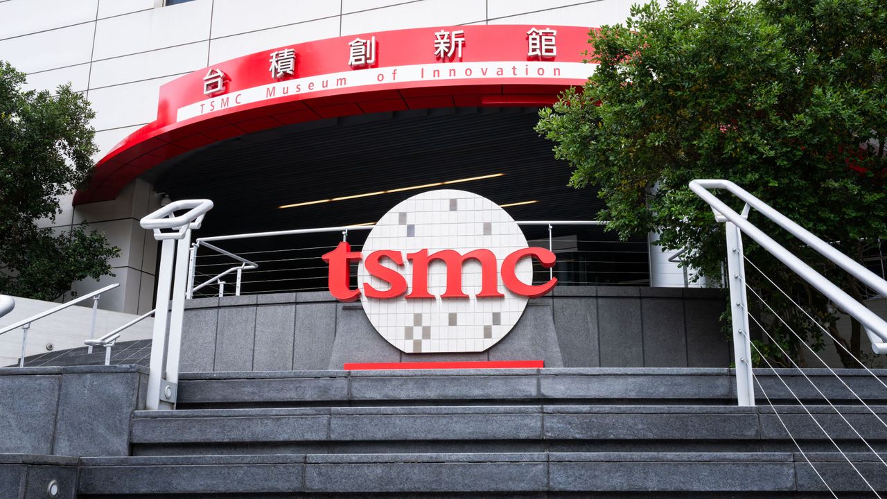
TSMC is executing the largest manufacturing expansion in semiconductor industry history that combines simultaneous multi-fab N2 ramps, AI-driven manufacturing optimizations, and massive CoWoS/SoIC packaging capacity expansion to meet increasing demand for AI accelerators.
TSMC says it does not have enough capacity to handle all the demand from AI hyperscalers, with CEO C.C. Wei saying that it will take a long time before it can match customer demand. This is an opportunity for Intel, though, as companies desperate to get their hands on advanced chips might be willing to use Intel 18A or 14A nodes for their needs instead.
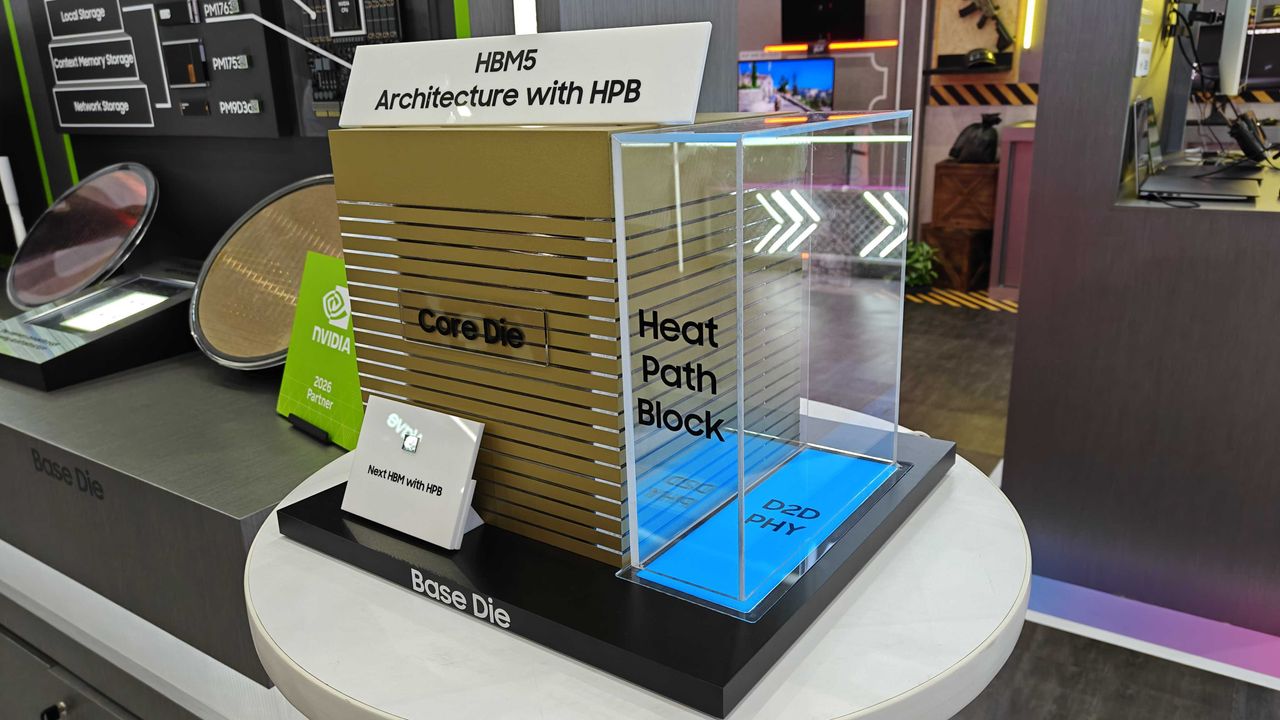
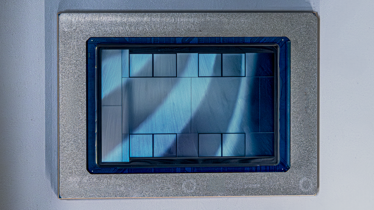
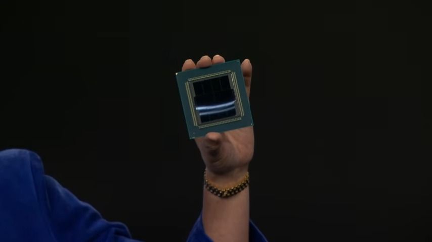
Samsung displayed its first physical mockup of HBM5 memory at Computex 2026 in Taipei, pairing the eighth-generation AI memory with a new in-package cooling structure.
We explore Globalfoundries, UMC, and SMIC's individual trailing-edge roadmaps, as each company is pursuing a fundamentally different strategy shaped by geography, regulation, and technology choices.
The certifications are valid for three years and were issued jointly by the China Information Technology Security Evaluation Centre and the National Secrecy Science and Technology Evaluation Centre.
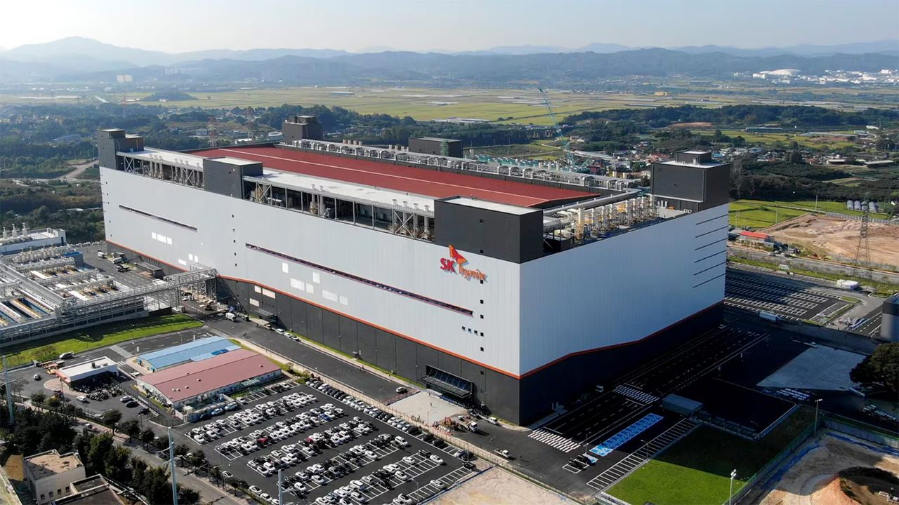
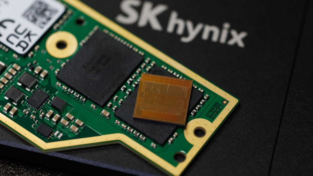
SK hynix has unveiled iHBM, a new thermal packaging architecture that embeds cooling elements directly into the HBM interface layer, reducing thermal resistance by 30% and helping future AI accelerators avoid performance-killing thermal throttling.
Imec unveiled the world’s first silicon quantum dot qubit device fabricated with High-NA EUV lithography, suggesting quantum computing may eventually scale using the semiconductor industry’s existing advanced manufacturing ecosystem.
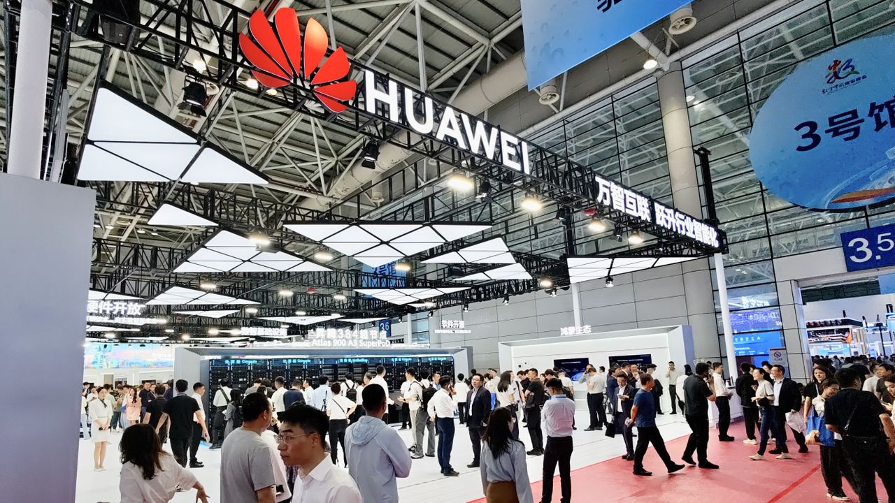
Huawei Technologies unveiled a new “LogicFolding” chip design framework built on its proprietary Tau scaling law, claiming it can dramatically boost transistor density and power efficiency without EUV lithography — potentially helping China narrow the gap with TSMC and Nvidia despite U.S. sanctions.
ASIC-based AI server shipments are projected to reach 27.8% of the market in 2026, the highest share since 2023, and custom ASIC shipments will grow 44.6% year-over-year.
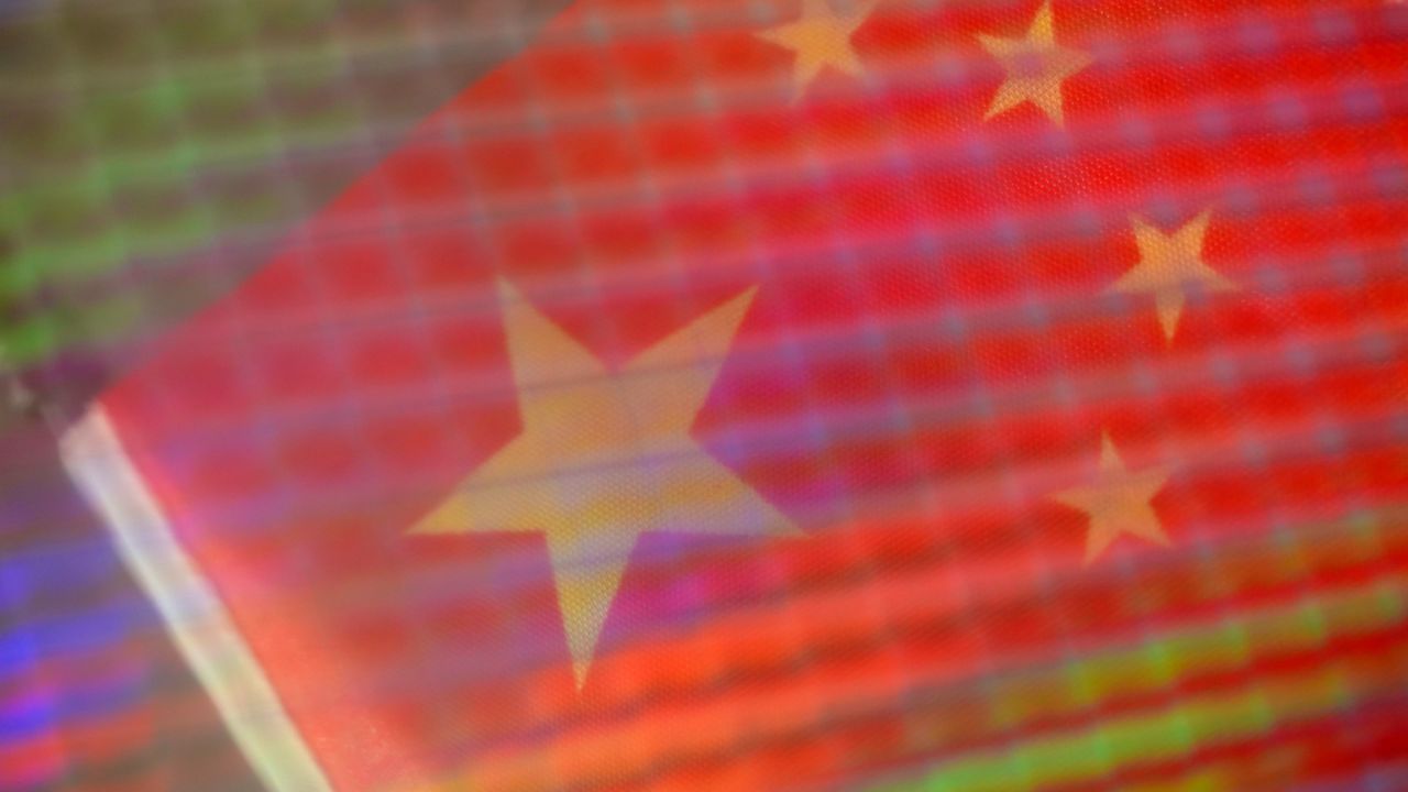
China's semiconductor equipment vendors collectively posted record revenues in 2025, but profitability is under pressure from domestic price competition.