❌

Lese-Ansicht

Tower Semiconductor to invest $4 billion in Japanese ops to set up massive optical connectivity hub

Tower Semiconductor and the government of Japan plan to co-invest a total of $4 billion in the company's Japanese operations to turn regional fabs into a massive manufacturing base for optical-connectivity semiconductors, reports Nikkei. The dual-track expansion will repurpose an idled fab, maximize output of an existing 300mm facility, and eventually add another 300mm fab, thus boosting Tower's Japanese capacity to the equivalent of 45,000 300mm wafers per month by 2029.

Track One: Convert and expand

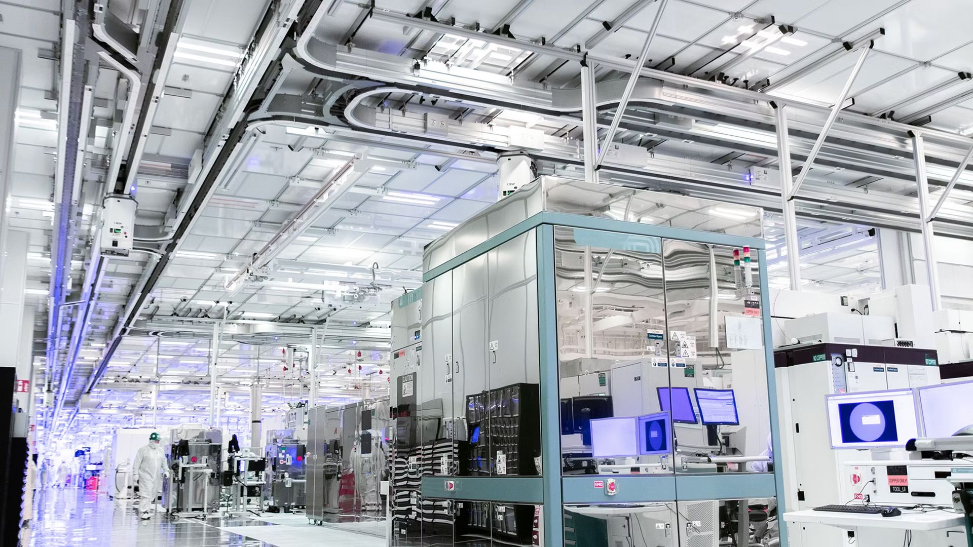
The first stage, called Track One, involves converting Tower's idle 200-mm Fab 6 in Arai, Niigata Prefecture, into a 300mm manufacturing facility for silicon photonics (SiPho) and advanced optical packaging (i.e., bonding electronic integrated circuits with photonic integrated circuits), as well as expanding the output of SiGe EICs (Silicon-Germanium Electronic Integrated Circuits) and SiPho PICs (Photonic Integrated Circuits) at 300-mm Fab 7 near Uozu, Toyama Prefecture.

Fab 7 is already fully qualified and is in mass production of various SiGe EICs and SiPho PICs using various process technologies, including the latest TPS65SG and several other TPS65-series 65nm-class SiGe fabrication nodes, as well as TPS45PHD 45nm-class SiPho manufacturing technology. The plan is to expand Fab 7's output as significantly as possible to meet growing demand for optical engines by the AI industry. Such an approach enables the company to add output progressively as additional equipment is installed, rather than waiting for an entirely new fab and process flows to qualify.

Track One is scheduled to reach full production readiness in the fourth quarter of 2027. Tower expects Track One to enable it to earn approximately $3.6 billion in revenue and $1.2 billion in net profit in FY2028.

Track Two: Build new fab

The second stage, called Track Two, commences in parallel and is considerably more ambitious. Tower intends to construct another 300mm manufacturing facility next to Fab 7 in Uozu that will increase the company's output of SiGe EICs and SiPho PICs by several times. As a result, Tower will have two sites in Japan producing EICs and PICs and one — the converted Fab 6 — assembling optical engines using these components.

The second stage is expected to start contributing materially to Tower's financial results in 2029.

Tower expects its Japanese production capacity to ultimately reach the equivalent of 45,000 300mm wafers per month in 2029, around 40 times higher than 2025 levels, and plans to hire approximately 200 people. The scale of the project reflects rapidly growing demand for optical connectivity in AI infrastructure. According to Nikkei, Tower controls more than 80% of the contract production market for optical communications semiconductors used in servers and serves some of the industry leaders, including Marvell, so it needs massive scale.

Tower plans to invest $3 billion of its own money in its two expansion tracks, while Japan's Ministry of Economy, Trade and Industry (METI) will provide another $1 billion, bringing the overall project to roughly $4 billion.

Tower admits that companies like Intel, TSMC, and GlobalFoundries are currently ahead in co-packaged optics (CPO), so the Japanese investment is not merely about adding capacity, but also about setting the stage for its CPO plans. For now, Tower intends to bring CPO and preceding manufacturing technologies to its Uozu, Toyama Prefecture, site. While the company has not disclosed any details about its CPO roadmap, even its latest process technologies for EICs and PICs should be more or less good enough to bring optics closer to compute silicon.

Tower's Japan restructuring

Tower Semiconductor's plans for major expansion in Japan also coincide with a restructuring of the company's local manufacturing operations. But understanding what is changing requires a short history lesson.

Tower established its Japanese manufacturing presence in 2014 by forming TowerJazz Panasonic Semiconductor Co. (TPSCo) with Panasonic, owning a 51% controlling stake while Panasonic retained 49% and contributed its fabs in Uozu, Tonami, and Arai. Following Panasonic's exit from the semiconductor business in 2020, Panasonic's stake passed to Nuvoton Technology Corporation Japan (NTCJ).

The most important asset is Fab 7 in Uozu, a 300mm facility that Tower has gradually transformed from a former Panasonic fab into one of its key specialty manufacturing sites that now supports 65nm-class SiGe and 45nm-class SiPho technologies.

Tower and Nuvoton are now effectively dismantling the original TPSCo structure. Under an agreement announced in March 2026 and expected to close in April 2027, Tower will take full ownership and operational control of Fab 7 and its 300mm foundry business, while Nuvoton will take full ownership of TPSCo and Fab 5 in Tonami. At the same time, Tower is resurrecting the former Arai facility, Fab 6, as a 300mm SiPho and advanced optical packaging site and plans to build another 300mm fab adjacent to Fab 7.

In short, what started as a relatively inexpensive way for Tower to obtain Japanese manufacturing capacity from Panasonic more than a decade ago is now evolving into a major Tower-owned 300mm SiPho and SiGe production hub, which is set to increase the company's output and revenue by multiple times.
  •  

Intel expects 14A to be 'within 5%' the performance of TSMC's A14

Intel's 14A (1.4nm-class) process technology is expected to deliver performance 'within 5%' of TSMC's A14 (1.4nm-class) production node, Naga Chandrasekaran, the chief technology and operations officer as well as general manager of Intel Foundry, told investment banking firm KeyBanc (via @Alex_Intel_). Given TSMC's track record of delivering steady performance, power, and area (PPA) gains with every new node, this might sound like entirely good news. However, the statement deserves a closer examination.

Delivering 'within 5%' performance is an ambiguous statement that may mean that 14A will be 5% faster than A14, or that 14A will be 5% slower than A14. While 'within 5%' performance compared to the direct rival of the same class may sound like a good competitive position, in recent years Intel's process technologies trailed TSMC's nodes in transistor density and remained competitive in performance or power. This was, to a large degree, attributed to Intel's historic focus on CPU performance, but not necessarily transistor density, as its own fabs have offset additional costs associated with larger dies.

In fact, actual shipping processors suggest Intel's 18A is at least competitive with TSMC's N2 in maximum achievable CPU frequency as Intel's Core Ultra X9 388H 'Panther Lake' can hit 5.10 GHz (at an 80W max turbo power), AMD's EPYC 9586F has the highest single-core clock of 5.0 GHz (at a default 500W CPU power), Apple's A20 Pro can achieve 4.93 GHz, whereas Apple's M6 can hit 4.78 GHz. These numbers should not be converted directly into a statement such as '18A is X% faster than N2,' because the processors use different architectures, voltages, standard-cell libraries, thermal envelopes, and physical implementations. However, they do provide a useful real-world reference point: the available N2 processors do not show a substantial frequency advantage over 18A. If anything, the highest observed CPU frequencies favor Intel's process.

Based on internal estimates, Intel officially states that compared to its already fast 18A, its 14A is expected to provide 15% – 20% higher performance at the same power, or 25% – 35% lower power at the same frequency and transistor count. By contrast, TSMC expects its A14 to be 10% - 15% faster than N2 at the same power, or 25% - 30% lower power at the same clocks and transistor count.

Combining the observed 18A and N2 CPU frequencies of Intel's 18A and TSMC's N2 with Intel's stated 15% – 20% 14A gain and TSMC's assumed 10% – 15% A14 gain would ordinarily suggest a modest 14A performance advantage of A14 even in most conservative scenarios for Intel. Therefore, Intel's new expectation that 14A will be 'within 5%' of A14 is notably less ambitious than one might infer from the company's published process specifications, even though the 'within 5%' statement does not tell us which process Intel expects to lead.

In fact, advantages of Intel's 14A over TSMC's A14 can be calculated using the highest observed 18A and N2 CPU clocks combined with Intel's and TSMC's official iso power performance projections.

Scenario

Intel 14A gain vs. 18A

TSMC A14 gain vs. N2

14A extrapolation from 5.10 GHz

A14 extrapolation from 5.00 GHz

Implied 14A advantage

Intel worst
TSMC best

15%

15%

5.865

5.75

2.00%

Both minimum gains

15%

10%

5.865

5.5

6.60%

Both maximum gains

20%

15%

6.12

5.75

6.40%

Intel best
TSMC worst

20%

10%

6.12

5.5

11.30%

Starting points: Intel 18A = 5.10 GHz (Core Ultra 9 388H); TSMC N2 = 5.00 GHz (EPYC 9586F).

With Intel’s Core Ultra X9 388H and AMD’s EPYC 9586F as the starting points, the official iso-power performance projections imply a 2% – 11.3% potential performance advantage for 14A over A14, depending on the combination of process-performance assumptions.

Scenario

Intel 14A gain vs. 18A

TSMC A14 gain vs. N2

14A extrapolation from 5.10 GHz

A14 extrapolation from 4.788 GHz

Implied 14A advantage

Intel worst
TSMC best

15%

15%

5.865

5.506

6.50%

Both minimum gains

15%

10%

5.865

5.267

11.40%

Both maximum gains

20%

15%

6.12

5.506

11.20%

Intel best
TSMC worst

20%

10%

6.12

5.267

16.20%

Starting points: Intel 18A = 5.10 GHz (Core Ultra 9 388H); TSMC N2 = 4.78 GHz (Apple M6).

Using Apple's M6 as the real-world N2 reference, a similar calculation gives Intel 14A a 6.5% – 16.2% implied advantage over TSMC A14. Even the worst possible combination for Intel — 14A achieves only +15% while A14 achieves the full +15% — puts Intel's node well beyond the 'within 5%' estimate given by Naga Chandrasekaran.

It should be clearly noted that our calculations do not predict 14A or A14 CPU frequencies, as we use clocks from current CPU architectures with improvement claims for upcoming process technologies. The calculation is useful primarily for illustrating what the companies' published numbers imply relative to today's products.

Intel's 'within 5%' assessment raises an interesting question: why does Intel expect 14A and A14 to be so close when the companies' published process gains appear to suggest a larger gap? Perhaps Intel's assessment incorporates factors that these simple calculations do not capture. Or perhaps the head of Intel Foundry took a page from his boss Lip-Bu Tan's book and now prefers to underpromise.

  •  

Leading semiconductor analyst says AMD should be investigated for 'treason' over availability of restricted chips in China

A Chinese tech firm’s crowd-funded project has touched off a firestorm over U.S. export controls after an analyst spotted a heavily restricted, military-grade AMD chip in its design selling for pennies on the dollar. The discovery — and the analyst’s subsequent call for a treason investigation — puts a sharp spotlight on how easily dual-use silicon can bypass strict U.S. national security sanctions through third-party supply chains ... despite corporate denials of direct sales.

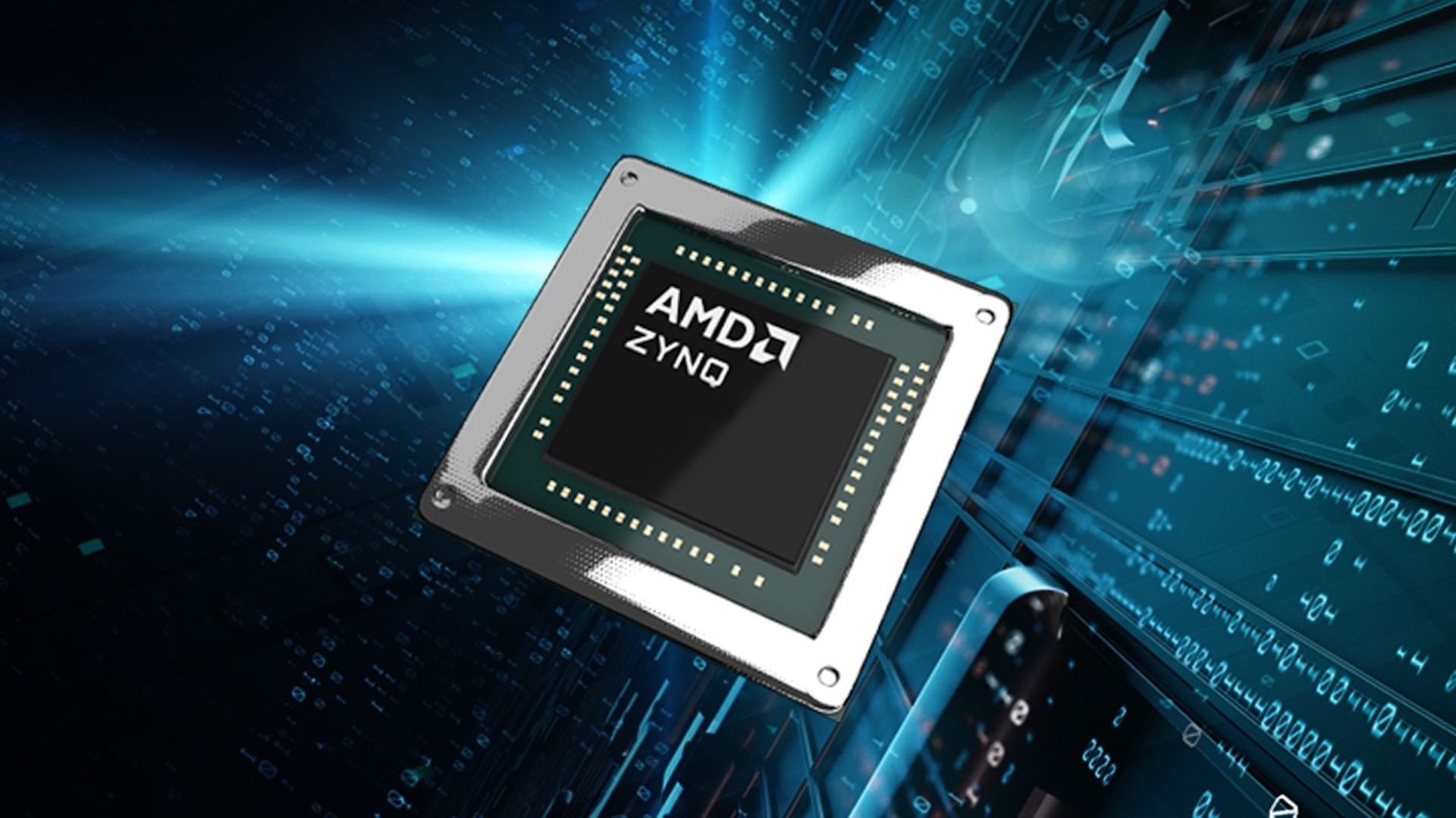
Dylan Patel, the head of top semiconductor analysis company SemiAnalysis, has discovered that China's Puzhi Electronic Technology is crowdfunding development of a system based on AMD's Zync UltraScale+ XCZU47DR RFSoC, which is a U.S. export-controlled dual-use component. He called on the government to investigate AMD for treason.

"AMD found a business opportunity in dumping U.S. military chips for ¼ of the cost in China," Patel wrote in an X post. "U.S. list price is $36K for this chip, with $4K – 5K to U.S. companies at volume, but it is getting quoted $1K in China to crowdfunding campaigns. AMD needs to be investigated for treason. It is not just export violations, but it is literally selling military end use components to an adversary for less than your home country."

In a statement to Tom's Hardware, AMD denied selling or shipping the chips directly into the restricted region. The company says it investigates suspected diversion cases to determine whether any violation of law occurred, although it did not explicitly confirm that it had opened an investigation into this particular case.

AMD needs to be investigated for treason

Dylan Patel, head of SemiAnalysis

"AMD is committed to full compliance with all U.S. and global export regulations and has a clear policy requiring our distributors, resellers, and customers to do the same," a spokesperson told Tom's Hardware. "Any shipment into restricted regions is a direct violation of our policy. This recent instance is unrelated to any direct AMD sales or shipments. We investigate all suspected diversion cases and if we find any violation of law, we will report it to relevant authorities and cease all business with the company."

AMD told Patel the same, according to another X post he made as a follow-up on the matter.

AMD's Zynq UltraScale+ XCZU47DR RFSoCs pack four general-purpose Arm cores, two Cortex-R5F real-time cores, an FPGA with 930,000 gates, and DSP engines with 4,272 DSP slices. It also has eight 14-bit analog-to-digital converters (ADC) capable of up to 5 GSPS and eight 14-bit digital-to-analog converters (DAC) operating at up to 9.85 GSPS to receive, process, and generate RF signals in real time without relying on separate data converters.

Devices based on Zynq UltraScale+ RFSoCs are used for software-defined radios, radar and phased-array systems, wireless and satellite communications, electronic test equipment, and other applications that require high-bandwidth, low-latency signal processing. Puzhi Electric officially positions its upcoming systems based on the Zynq UltraScale+ RFSoCs for 'professional engineers' and 'advanced researchers in universities,' though such systems can be used for completely different applications.

AMD's Zynq UltraScale+ XC-series RFSoCs are designed for commercial and industrial applications, but AMD also offers separate XQ-series defense-grade RFSoCs for aerospace and defense applications, although there the XCZU47DR does not have a direct XQZU47DR counterpart. Yet, the closely related ZU48DR is available in both XC and XQ versions. The latter adds defense-oriented qualification, ruggedization, and support rather than fundamentally different processing capabilities.

Therefore, while the XCZU47DR is technically aimed at civil, commercial, and industrial applications, the chip is a dual-use component featuring a 3A001.a.14 ECCN classification under the U.S. Commerce Control List (CCL) and therefore its exporting, re-exporting, or transferring normally requires a BIS export license to non-allied destinations (e.g., China) on anti-terrorist and national security concerns. This means that any shipment to China requires a license, but in practical reality, that license will almost certainly be denied. However, there is a license exception that allows shipping such items to commercial companies from the Group B countries, which means legitimate exports to dozens of states from where such goods could get to China illegally.

This might explain how Puzhi obtained its XCZU47DR devices, but it does not explain the enormous apparent difference between the prices available to Chinese and American buyers. The $1,000 figure, however, is Patel's reported price for the chip rather than a publicly advertised retail offer.

Xilinx, which AMD later acquired, introduced its 3rd Generation Zynq UltraScale+ RFSoC family, including the XCZU47DR, in February 2019, and the devices reached production status in 2020, meaning that they have been on the market for almost six years now. Xilinx and then AMD have sold the unit to tens, if not hundreds, of companies in different countries, so determining the origin of the units that Puzhi has might be difficult.

It should be noted that lead times for XCZU47DR at various resellers like Avnet and DigiKey are 40 to 52 weeks, which indicates that the components are in high demand in the U.S. and Europe. Meanwhile, Puzhi claims it can ship its system based on the RFSoC on November 6, 2026.

  •  

ASML says it sold 'absolutely nothing' in Europe in 2026

As the world's only supplier of EUV lithography systems, ASML is Europe's largest company by market capitalization, currently valued at around $660 billion. But it earned almost nothing in Europe this year, down from 1% of total profits in 2025 and 5% in 2024. Why? European chipmakers bought no lithography equipment from ASML in 2026 — and the company is calling on EU authorities to help create demand for European chips.

"We are selling absolutely nothing in Europe," said Frank Heemskerk, executive vice president of public affairs at ASML, while speaking at a panel discussion from the Dutch political and cultural center De Balie. "Because Europe is not investing and because no chip factories are being built in Europe. That is genuinely worrying. […] [Our revenue share in Europe is 0%], it used to be 1%."

Indeed, Europe accounted for 1% of ASML's revenue share in 2025, 5% in 2024, 4% in 2023, and 2% in 2022, based on the company's presentations for investors. In the first two quarters of 2026, however, Europe accounted for 0% of ASML's revenue, according to ASML's earnings reports.

"There simply is no demand here for these kinds of highly specialized machines," Heemskerk said. "That is the problem. So apart from trying to attract investment with capital on the supply side, we should do much more to create demand. […] So, we at ASML are also making an enormous effort, and we are talking with Ursula von der Leyen in Europe, saying: 'try to harness the market power and dynamism that ultimately do exist in Europe in a number of areas.'"

So far, the European Union has been keen on subsidizing building new fabs in Europe (something that did not help to lure Intel in). But ASML is calling on European governments to help aggregate and guarantee demand for European-made chips — which will encourage major European chip consumers to source locally, giving semiconductor manufacturers an economic reason to build or expand fabs in Europe.

"We need to make sure that some of those buyers — the customers of our customers — start talking much more closely with European manufacturers again. In areas such as artificial intelligence for industry, for example, there are still plenty of opportunities that Europe can seize. But you have to organize this collectively."

New fabs are being built…

That said, the ASML EVP may be too pessimistic about Europe's semiconductor industry.

Intel runs its massive Fab 34 near Leixlip, Ireland, and recently announced plans to invest €5 billion in the facility to expand production of CPUs on Intel 4 and Intel 3 process technologies. While the new investment dwarfs Intel's plans to invest roughly €80 billion in its Magdeburg, Germany, fab complex, with two first fabs alone accounting for over €30 billion, it still represents Intel's commitment to its Ireland campus.

In addition, ESMC — which is backed by TSMC, Bosch, Infineon, and NXP — is building a brand-new fab near Dresden that will cost around €15 billion. The fab will be capable of producing chips using 12nm/16nm-class FinFET and 22nm/28nm planar transistor-based process technologies used in a wide range of automotive applications. The same nodes are also used for various consumer electronics and edge applications.

Infineon also opened its new €5 billion Smart Power Fab in Dresden in July 2026, which marked the largest single investment in the company's history and effectively doubled its manufacturing capacity at the site. The 300mm facility produces power semiconductors as well as analog and mixed-signal chips for automotive, industrial, renewable-energy, and AI data-center applications.

Last but not least, GlobalFoundries officially broke ground on the latest major expansion and upgrade of Fab 1 in Dresden this March to increase capacity for its specialty process technologies, including 22nm FD-SOI (22FDX), embedded non-volatile memory (eNVM), and the BCD (bipolar-CMOS-DMOS) node for power management ICs. To some degree, the upgrade was forced by headwinds that GlobalFoundries faced when building the €10.4 billion joint fab with STMicroelectronics in the Grenoble, France, region.

With numerous semiconductor fab projects in place in Europe, ASML will continue to sell its tools to companies in the EU for years to come; the semiconductor industry is far from dead in the bloc. Of course, the important detail is that all of these production facilities are built by multinational corporations (sometimes in collaboration with local companies) — but this is largely a global trend rather than a major issue.

…But there's a catch

Although the fab projects in Europe are large in terms of investment, they pale in comparison with those being built in Taiwan, South Korea, the U.S., and Japan, where tens or even hundreds of billions of dollars are being invested in new semiconductor production facilities.

What is perhaps more important from ASML's standpoint is that none of the ongoing fab projects in Europe are leading-edge fabs set to use EUV and eventually High-NA EUV lithography scanners. The tools that European fabs use today and that new facilities are set to use in the future are mature tools that cost considerably less than advanced EUV or immersion DUV scanners. This is perhaps a concern for ASML, as the company is naturally interested in selling its more sophisticated and expensive equipment.

Another concern is that even advanced silicon produced in Ireland or at ESMC is then shipped to other regions for packaging, meaning that European companies have largely lost their ability to produce sophisticated chips entirely in Europe. In turn, this means that, for now, there is hardly any strategic point for European authorities to create demand for chips that are 'Made in Europe' because they are either not assembled in Europe, not produced in Europe, or not developed in Europe. We have no idea whether this is eventually going to change, but there are currently no signs that it will.

  •  

AMD begins to add GDDR7 support to its Linux GPU drivers

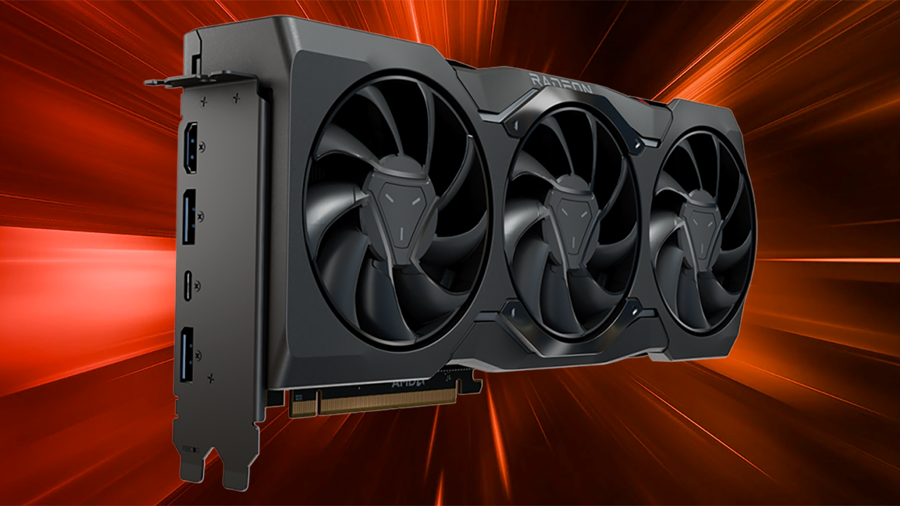
AMD has started to add support for GDDR7 memory and several new graphics IP blocks to its open-source Linux kernel driver, which indicates that software enablement for the company's next-generation standalone GPUs is underway, reports Phoronix. While AMD does not identify the upcoming architecture, the changes are likely tied to its RDNA 5 project — but they don't necessarily herald an imminent launch.

AMD's existing Radeon RX 9000-series graphics processors based on the RDNA 4 architecture use GDDR6 memory, so the addition of GDDR7 identification to drivers is arguably the most explicit confirmation that AMD is setting the stage for its next-generation discrete Radeon graphics processors based on the RDNA 5 architecture.

AMD also submitted patches that enable IH 8.0, a new version of its Interrupt Handler IP block, as well as NBIF 7.10, the latest revision of the company's New Bus Interface. Several smaller patches make additional preparations for the new hardware. These changes follow earlier Linux driver work involving Display Core Next 6 (DCN6) as well as GFX 13.0.x, suggesting that AMD is gradually upstreaming support for multiple components of an upcoming GPU architecture. Yet, while enablement of IH8, NBIF 7.10, DCN6, and GFX 13.0.x clearly point to new graphics hardware, it does not necessarily point to new discrete GPUs, unlike the mention of GDDR7.

As revealed in August, 2025, Laks Pappu, Senior Fellow at AMD, is the lead architect for AMD's next generation datacenter GPU and discrete graphics platforms. Pappu was building next-generation "competitive 2.5D/3.5D chiplet-based and monolithic graphics SoCs on various packaging technologies," according to his LinkedIn profile before it was edited to remove those disclosures.

Essentially, Pappu's profile indicated that AMD's next-generation GPU architecture could support multiple physical implementations — including multi-chiplet and monolithic — depending on performance, cost, market requirements, and AMD's willingness to compete in certain market segments

AMD has already used a multi-chiplet design with its Navi 31 GPU, an implementation that kept graphics processing hardware on a large Graphics Compute Die (GCD), but disaggregated memory interfaces and caches into smaller Memory Cache Dies (MCDs). A more ambitious implementation could potentially distribute graphics processing resources between multiple dies, although Pappu's profile did not disclose how AMD intended to partition its future GPUs.

Such an approach would be considerably more complicated than separating memory and cache functionality. Multiple compute dies would require high-bandwidth, low-latency connections as well as mechanisms for synchronization and coherency, while software would ideally continue to see the set of chiplets as a single graphics processor.

Based on conventional GPU development cycles of roughly 2.5 to 3.5 years, RDNA 5 could already have been approaching tape-out or early post-tape-out stages when the information surfaced in August 2025, which means that the company is already likely to be testing the new GPUs internally.

Officially, AMD hasn't disclosed any details about its RDNA 5 architecture nor launch schedule, so take these developments with a grain of salt. For now, all we know for sure is that AMD is working on standalone RDNA 5-based GPUs, and they're likely to use GDDR7 in at least some configurations, assuming the AI-driven memory crunch doesn't choke supply of those chips even further for consumer applications.

  •  

Memory chips are now more expensive than compute chips on a per-area basis

Memory prices are at record highs due to demand from the AI sector and are not going to drop any time soon. In fact, the cost of manufacturing memory chips on a per-area basis can be higher than the price of silicon processed using TSMC's N2 and N3 fabrication technologies, which are used to make compute chips, according to an observation made by Kurnal Insights. While the comparison has merit, it has an important caveat.

DRAM Wafer price is more expensive than TSMC N3 Wafer Price pic.twitter.com/uWqizOZ6iGSeptember 20, 2026

Based on media leaks, Kurnal from Kurnal Insights considers that a 300-mm wafer processed using TSMC's N3 technology costs $20,000, which translates to approximately $0.283 per mm² when the wafer price is divided by its area. For TSMC's N2, the analyst assumes a considerably higher wafer price of $30,000, or around $0.424/mm². These calculations are based on unofficial information and do not account for unusable wafer edges, dicing, test structures, defects, or yield, so they should be viewed as nominal wafer-area prices rather than the actual price of usable silicon.

The calculation for DRAM works differently. Kurnal assumes a DRAM price of $1.50 per Gb and then multiplies it by the bit density of different generations. At 0.219 Gb/mm², 1y DRAM works out to $0.329/mm², whereas 1z DRAM with its 0.273 Gb/mm² density reaches $0.410/mm². Finally, 1b DRAM at 0.436 Gb/mm² produces a figure of $0.654/mm², considerably higher than the nominal $0.424/mm² calculated for an N2 wafer.

There is an important distinction here. The N2 and N3 numbers represent assumed prices charged by TSMC for processing a wafer, whereas the DRAM figures represent the potential selling value of the memory contained within a square millimeter of silicon, thus illustrating how much revenue a DRAM maker can theoretically get from a given die area at the assumed memory price.

Interestingly, Kurnal Insights' $1.50/Gb assumption is almost exactly in line with the current spot price of DDR5 eTT memory. According to DRAMeXchange, 16Gb DDR5 eTT chips carried a session-average price of $24.80 on September 21, equivalent to $1.55/Gb. At that price, 1b DRAM with a density of 0.436 Gb/mm² would be valued at approximately $0.676/mm², just 3% above Kurnal's $0.654/mm² estimate.

It goes without saying that producing DDR5 memory is considerably cheaper than making logic chips using TSMC's N3 process technology. However, with DRAM in short supply, memory makers are getting considerably more money for their silicon than they did historically.

There are a few important caveats that make the comparison somewhat less straightforward. The calculations do not account for packaging costs, with logic requiring more expensive techniques. Additionally, TSMC manufactures chips on a contract basis, and the actual price of a processed wafer depends on the volumes, customer, and other commercial terms. Thus, comparing estimated TSMC wafer prices with DRAM spot prices is not exactly an apples-to-apples comparison. Even TrendForce notes that DDR5 spot procurement remains limited and transactions are sporadic, which means spot prices do not necessarily reflect the prices at which Micron, Samsung, and SK hynix sell the bulk of their DRAM.

Therefore, contract DRAM prices would provide a considerably better basis for an economically meaningful comparison. However, we do not know contract prices, and while they are clearly higher than historical memory prices, they may not be as high as spot prices. To that end, we cannot state for sure that DRAM makers get more money for their wafers than TSMC does for its logic wafers.

  •  

China's CXMT hits 12nm-class DRAM milestone

China's DRAM champion CXMT has begun mass production using its 5th-generation DRAM process technology.

CXMT says its new process technology — G5, as the company calls it — reduces DRAM’s active-area half-pitch to 11.95nm using quadruple-patterning lithography. The 11.95nm half-pitch corresponds to an active-area pitch of 23.9nm, something that puts this particular dimension roughly in the range of other advanced 10nm-class DRAM technologies. However, it cannot be directly translated into a conventional DRAM node designation. Separately, CXMT says its DRAM-optimized high-K metal gate (HKMG) process reduced the height of the core cell array to 6,762nm.

The company also says it modified its process flow and introduced unspecified new materials to enable storage capacitors with a depth-to-width aspect ratio of about 45:1.The figure is certainly difficult to compare directly with competing DRAM process technologies, but SK hynix says that capacitor aspect ratios will need to exceed 100:1 as DRAM critical dimensions eventually fall below 10nm.

A 45:1 aspect ratio means CXMT’s storage capacitors are 45 times deeper than they are wide, which is what enables the company to reduce DRAM cell area and fit more memory arrays onto a wafer and retail predictable capacity. However, increasingly high aspect ratios make etching, deposition, mechanical stability, and ultimately high-yield manufacturing considerably more challenging.

The first disclosed mass-produced devices using G5 are said to be 24Gb LPDDR5X devices, which have already entered mass production. The chips offer 50% more capacity than CXMT's previous comparable products and are available in two package formats for different mobile-device designs. According to the Chinese report, the 24Gb LPDDR5X products are already entering mainstream Chinese flagship smartphones.

A nanometer caveat?

Meanwhile, there are some important caveats.

First up, CXMT's 11.95nm figure represents the active-area half-pitch rather than a conventional process-node designation, so calling G5 a 12nm process is a large degree of simplification at best.

Secondly, the two revealed physical dimensions do not mean technological parity with the latest DRAM processes from Micron, Samsung, and SK hynix, as density, capacitor scaling, transistor characteristics, power consumption, and, arguably most importantly when it comes to commodities, yields matter.

Thirdly, CXMT says G5 provides at least 50% more gross dies per wafer than G4, but without actual numbers, this is obsolete. CXMT also did not disclose yields, which makes it impossible to determine the increase in productivity, not to mention known-good dies or the actual manufacturing cost per bit. Yet again, even a claimed 11.95-class DRAM node is an achievement.

  •  

Huawei shelves global AI chip rollout as China's own demand outstrips supply

Huawei's impressive next-generation Ascend 900-series AI accelerators will be offered only in China, not internationally, as the company struggles to meet domestic demand amid capacity constraints, the company announced this week. While the upcoming Ascend 960-series neural processing units (NPUs) could rival some of AMD's and Nvidia's existing AI GPUs, demand for these units outside of China was not guaranteed anyway.

"Since we do not have enough capacity to even satisfy the ​demand in China, we do not have a plan to expand into the international market in a fully-fledged way," said Eric Xu, rotating chairman of Huawei, on the sidelines of the company's Huawei Connect conference, Reuters reports. He added that Huawei supplies limited volumes to 'some countries where demand is particularly strong,' though he did not elaborate.

Huawei this week unveiled its latest AI accelerator roadmap, revealing major training and inference performance gains for its next-generation Ascend 960, 970, and 980 NPUs over the existing Ascend 910C and Ascend 950-series. The Ascend 960DT and 960PR are set to increase their FP8 training performance to 2 PFLOPS and their FP4 inference performance to 4 PFLOPS and 8 PFLOPS, respectively, in 2027. Meanwhile, their successors, Ascend 970 and Ascend 980, are projected to increase their FP4 performance to 14 PFLOPS and 28 PFLOPS, respectively, in the coming years.

Huawei Ascend vs Nvidia AI GPUs

NPU

FP8 Performance

FP4 Perf

Memory

Memory Bandwidth

Interconnect Bandwidth

Targeted Release

Nvidia H200

4 PFLOPS

-

141 GB HBM3E

4.8 TB/s

900 GB/s

2023 Q4

Nvidia B300

10 PFLOPS

15/20 S/D PFLOPS

279 GB HBM3E

8 TB/s

1.8 TB/s

2025 Q4

Ascend 950PR

1 PFLOPS

2 PFLOPS

128 GB of HiBL 1.0

1.6 TB/s

2 TB/s

2026 Q1

Ascend 950DT

1 PFLOPS

2 PFLOPS

144 GB of HiZQ 2.0

4.0 TB/s

2 TB/s

2026 Q4

Nvidia R200

17.5 PFLOPS

35/50 T/I PFLOPS

288 GB HBM4

19.2 TB/s

3 TB/s

2026 Q4

Ascend 960DT

2 PFLOPS

4 PFLOPS

288 GB

9.6 TB/s

2.2 TB/s

2027 Q1

Ascend 960PR

2 PFLOPS

8 PFLOPS

192 GB

2.4 TB/s

2.2 TB/s

2027 Q3

Ascend 970

3.6 PFLOPS

14 PFLOPS

288 GB

14.4 TB/s

4.4 TB/s

2028

Ascend 980

7.2 PFLOPS*

28 PFLOPS*

384 GB

38.4 TB/s*

8 TB/s

2029

*Preliminary data
S/D - Sparse and Dense
T/I - Training and Inference

But while the upcoming Ascend NPUs will be considerably faster than their predecessors, particularly for inference, they will remain well behind Nvidia's previous- and current-generation accelerators, at least in raw compute performance. Huawei's 2027 Ascend 960DT is projected to deliver 2 FP8 TFLOPS for training, compared with Nvidia's 4 FP8 TFLOPS for the H200, released in 2023. The Ascend 960PR is expected to offer 8 FP4 PFLOPS for training, which is far behind Nvidia's B300, which delivers 15–20 NVFP4 PFLOPS. Even the Ascend 980, targeted for 2029, is projected to reach 7.2 FP8 PFLOPS and 28 FP4 PFLOPS, well below Nvidia's R200, which is on track to deliver 17.5 FP8 PFLOPS and 35/50 FP4 PFLOPS this year.

Such a massive performance difference with leading AI hardware will reinforce Huawei's reliance on massive system-level scaling rather than chip-for-chip performance to compete with Nvidia. But massive system-level scaling comes with massive power consumption, which will make Huawei's next-generation Atlas SuperPoDs and SuperClusters considerably less competitive in markets that can access hardware from AMD or Nvidia.

Huawei is in an interesting paradoxical situation. On the one hand, its integration efforts like near-package optics (NPO) clearly free up capacity on 'older' nodes that can be used for other components of AI platforms. But on the other hand, SMIC's inability to ramp production on 7nm and 6nm-class nodes limits Huawei's ability to supply its AI hardware anyway, which is why it can barely meet demand.

Then again, while Huawei's Atlas SuperPoDs with up to 15,488 Ascend 960 NPUs can deliver up to 30 FP8 EFLOPS and 120 FP4 EFLOPS performance by far exceeding the capabilities of Nvidia's NVL72 clusters with a 72-GPU scale-up world size, their performance-per-watt is poised to be dramatically lower compared to Nvidia's architectures, which means that demand for such hardware outside of China will be limited at best. That said, a global AI hardware push doesn't make much sense for Huawei right now. What perhaps does make sense is offering cloud access to its hardware to various academic and research customers to popularize its CANN software stack.

  •  

China crafts working 3nm gate-all-around transistors without EUV

The Institute of Microelectronics of the Chinese Academy of Sciences (IMECAS) has developed an experimental process flow for building stacked-nanosheet gate-all-around (GAA) transistors using immersion DUV lithography and demonstrated functional devices. The flow is intended for eventual use with 3nm-class and smaller process technologies by Chinese chipmakers that do not have access to EUV scanners, reports DigiTimes.

While IMECAS has demonstrated functional GAA devices, it has not disclosed the critical geometrical parameters that would allow comparisons to 3nm-class transistors from other chipmakers. Furthermore, the experimental process flow for building transistors is not even a defined process flow for building research chips, much less a complete 3nm-class manufacturing process.

Nonetheless, the achievement is quite important as it demonstrates that China is capable of developing its own branch of semiconductor evolution without using leading-edge tools from Western companies.

Early process integration complete

Ye Tianchun, chief engineer of China's National Major Special Project 02, said at the IC World conference in Beijing that IMECAS had completed 'early process integration' for stacked nanosheet-channel GAA transistors fabricated with DUV lithography. The researchers from IMECAS obtained devices with Ion/Ioff ratios of 9.7×10⁵ and 7.6×10⁵, both exceeding the 5×10⁵ threshold, which means gate control of the stacked sheets is working. These figures indicate that the experimental transistors can distinguish between their conducting and non-conducting states, but they say little about transistor density or whether their physical dimensions correspond to those expected from commercial 3nm-class technologies.

In particular, IMECAS has not disclosed gate pitch, metal pitch, nanosheet dimensions, transistor density, SRAM density, or other geometrical characteristics that could put its devices into perspective against 3nm-class production nodes from Intel, Samsung Foundry, or TSMC. Therefore, the achievement should be viewed as validation of a stacked-nanosheet GAA process flow based on DUV lithography rather than evidence that China has developed a 3nm process without EUV.

The most important part of the experiment is that IMECAS is investigating how GAA devices intended for future 3nm-class and more advanced technologies can be fabricated without using EUV lithography, something that nobody has done before in volume production.

GAA transistors have succeeded FinFET devices at leading-edge nodes because placing the gate around nanosheet channels provides better electrostatic control as transistor dimensions shrink. IMECAS has been developing technologies required for this transition since 2020, and its particular focus was on nodes below 3nm, which is why it now mentions 3nm as part of its announcement.

Reducing China's dependence on advanced foreign tools

It goes without saying that IMECAS' work in recent years has been focused on reducing China's dependence on tools, software, and other technologies that are designed by Western companies and therefore subject to export restrictions imposed by American, Japanese, or European countries.

Among other things, Ye mentioned architectural innovation, design-technology co-optimization (DTCO), system-technology co-optimization (STCO), and 'extracting more value' from mature fabrication technologies. For now, IMECAS' result demonstrates a DUV-based route for researching stacked-nanosheet GAA transistors intended for future 3nm-class technologies, but not a China-developed 3nm process ready for manufacturing even in the long-term future.

Even if IMECAS eventually demonstrates appropriately scaled GAA devices using DUV, or discloses critical geometry parameters of the current work, this would still be far from a production-ready 3nm-class technology. Commercial manufacturing requires integration of lithography with deposition, etching, cleaning, metrology, process control, materials, temperatures, and many other steps and parameters. For now, IMECAS has not demonstrated such a manufacturing flow.

  •  

OpenAI projections point to a massive $278 billion cash burn through 2030 that exceeds the national budgets of Indonesia and Norway

OpenAI expects to spend $278 billion more money than it generates between 2026 and 2030 due to aggressive spending on compute capacity and adjacent infrastructure, according to a recent presentation seen by the Financial Times. While the company projects nearly 10X revenue growth over the four-year period, the AI developer expects its spending on production capacity and supporting infrastructure to exceed its earnings by over a quarter of a trillion dollars.

OpenAI expects its revenue to increase from $36 billion in 2026 to $350 billion in 2030 and expects to book a total of $840 billion in revenue between now and the end of the decade, according to the presentation, which the company presumably sent to its current and potential investors ahead of its expected IPO. OpenAI plans to spend about $856 billion on computing resources and infrastructure over the same period, its largest expense.

The company also intends to spend an additional $262 billion on other things during the period. As a result, OpenAI forecasts cumulative negative free cash flow of $278 billion from 2026 through 2030. While the sum is massive, this represents an improvement from a projection made in May, when the company expected cumulative negative free cash flow of $305 billion, FT notes.

Financing OpenAI's continuous expansions requires huge amounts of additional capital. OpenAI raised $122 billion in March, but its current financial model indicates that this money could be depleted in 2028, FT reports. The company, recently valued at $852 billion, has already entered discussions about another large investment round. Prospective investors have approached OpenAI about providing capital at a valuation of $1.2 trillion, while a person close to the company said OpenAI is seeking an even higher valuation.

The spending reflects the gargantuan cost of building AI data centers and additional infrastructure to train new AI models and then use them to provide services to clients. Meanwhile, it means OpenAI's revenue growth will lag its spending so much that it will burn $278 billion in four years. To put it into context, $278 billion is only slightly below the Austrian government's $286 billion spending in 2024 and exceeds the annual government expenditures of Indonesia and Norway, at least according to the IMF.

To put the $278 billion figure into a perspective more relevant to OpenAI, it equals four years of $20 monthly subscription fees paid by roughly 290 million people. As of early 2026, OpenAI had over 50 million consumer subscribers (at different plans), over 9 million paying business users (again, at different prices per seat), and more than 900 million weekly active users.

OpenAI had planned an initial public offering for autumn 2026 and confidentially submitted documents to the U.S. Securities and Exchange Commission in June, but later postponed the process, citing increasing public concern about risks associated with rapidly advancing AI systems. Some experts also believe the delay reflects concerns about how public markets would value a company that generates losses that exceed the budgets of countries like Indonesia. Meanwhile, Anthropic is expected to pursue an IPO this autumn that could become the largest ever.

  •  

Jensen Huang says there is '0% chance' AI destroys the world by 2030 — 'We should go as fast as we can, irrespective of anyone else,' dismisses Anthropic doom warnings and rejects new regulations

Jensen Huang, the chief executive of Nvidia, said artificial intelligence will not destroy humanity by the end of the decade, Bloomberg reports, citing a CBS interview. Huang contends that while AI is developing at an extremely rapid pace, doomsday scenarios because of AI are largely unsubstantiated, and it makes no sense to 'stir fear across America.'

"I completely disagree that AI will destroy the world by 2030," Huang said in an interview with CBS Sunday Morning (set to be aired on Sunday).

"I believe the claims of the end of the world, stirring fear across America, and doing it by people who are doing it makes no sense to me. So, they must be doing it for ulterior reasons. Maybe it is political, maybe it is otherwise, maybe it is just attention-grabbing […]. However this is characterized, 2030 is not going to be the end of the world. There is 0% chance that is going to be the end of the world."

Huang, who leads the company that leads the market in AI hardware sales, is responding to Evan Hubinger, the former Alignment Science organization lead at Anthropic, who said there was an over 10% chance that AI would destroy humanity within the next decade.

"We really do earnestly believe AI could kill all humans," Hubinger wrote in an X post. "I personally think it is >10% within the next decade. I believe Anthropic is trying its best, but we do not yet have a plan to solve alignment for superintelligence and are not clearly on track to."

Following reports that OpenAI's rogue agents attacked Hugging Face and communicated with each other on abandoned wikis and websites, chief executives of Anthropic and OpenAI called for guardrails and even slowing down development of new AI models, as the dangers they pose are not completely evident even to their developers.

The head of Nvidia states that AI can be safely managed by its developers, so no regulations from governments are needed beyond what is already in place. Meanwhile, he also says that products shipped must be completely safe.

"We should go as fast as we can, irrespective of anyone else," Huang said. "But we would never ever, and never should, ship products before they’re ready and deliver products that are unsafe."

  •  

Elon Musk's Terafab hits a roadblock before making a single chip, receives cease-and-desist order — firm files trademark lawsuit, has sold Tera-Fab-branded lithography tools for over a decade

In an unexpected turn of events, Terafab has faced an odd roadblock as a small U.S.-based company called Tera-Print sent a cease-and-desist letter to SpaceX and Tesla back in May to stop using the Terafab name. The company with tera-scale ambitions has run into a tabletop-sized problem because the Tera-Fab name has already been used for about a decade by Tera-Print, according to PCMag.

As it turns out, Tera-Print sells tabletop-sized Tera-Fab-branded beam pen lithography (BPL) tools primarily aimed at bioengineering and prototyping of microfluidic devices and has used the brand for about a decade. The U.S. Department of Defense appears to be a client of Tera-print, which uses Tera-Fab.

While Tera-print claims that the Terafab name could be confused with its Tera-Fab product family, Tesla, SpaceX, and SpaceXAI counter that the operations are fundamentally different: Terafab is set to produce chips in extremely high volumes to serve AI, automotive, robotics, and eventually (at least some) space applications, whereas Tera-print's Tera-Fab is a compact lithography tool that can be used for bioengineering or prototyping of electronic or optical devices.

Formally, the trademark coverage puts both names into the same semiconductor technology bucket, albeit with different descriptions:

  • Tesla's Terafab covers 'custom manufacture of semiconductor chips, memory chips, integrated circuits, and wafers' (IC 040) as well as 'distribution services, namely, delivery of semiconductor chips, chip carriers, namely, semiconductor chip housings, memory chips, integrated circuits, semiconductors, and microchips' (IC 039).
  • Tera-print's Tera-Fab covers 'Polymer pen and beam pen lithography instruments in the nature of 3D micro-printers and 3D nano-scale printers' (IC 007); 'Polymer pen and beam pen lithography instruments in the nature of 2D micro-scale molecular and material printers and 2D nano-scale molecular and material printers' (IC 009), 'Light-directed photochemical synthesis tools; Industrial advanced materials synthesis tools; Advanced light projection systems; High precision force-feedback sample alignment modules; Environmental control sample chambers' (IC 009); as well as 'training services in the field of AI design and development, electronics, computer science, biology, and material science' (IC 042).

The two companies reportedly entered settlement talks, which included an offer from Tesla, but Tera-Print alleges that Tesla expressed interest in continuing negotiations instead of taking the dispute to court. Tera-Print says it will now defend its registered trademark and argues that the companies operate in related fields, which could lead to confusion.

  •  

China's premier memory maker CXMT eyes producing flash for SSDs, report claims — 3D NAND research and development line rumored for its second manufacturing facility near Beijing

A new report claims Chinese DRAM champion CXMT is eyeing production of 3D NAND memory. Reuters reports, citing three people familiar with the company's plans, that CXMT intends to build a 3D NAND R&D production line at its second manufacturing facility near Beijing. There is no information on when the experimental production line will become operational, though, given that CXMT's second Beijing fab has not even broken ground yet, the line is at least two or three years away. In addition, the memory maker has established a research institute in Beijing that has NAND flash development among its projects, according to one source. CXMT has not formally confirmed any 3D NAND initiatives, so the information should be taken with a grain of salt.

For now, there are no details on CXMT's 3D NAND architecture, number of active layers, process technology, expected performance, or production capacity. Nevertheless, the report claims that CXMT has already discussed its NAND ambitions with prospective customers. One of them is said to be a recently established company that plans to use CXMT-made NAND devices in storage products aimed at AI and supercomputing applications.

It remains to be seen whether CXMT's 3D NAND project will eventually progress to high-volume manufacturing, but if it does, the initiative will take CXMT beyond its traditional DRAM specialization and directly into YMTC's territory. Until recently, China's two major memory producers had focused exclusively on their 3D NAND and DRAM realms where they have achieved quite a success. Yet, it looks like both companies want to become one-stop shops for DRAM and NAND — just like their bigger rivals Micron, Samsung, and SK hynix — as YMTC is reportedly exploring DRAM production.

While CXMT's alleged plan to build 3D NAND may look somewhat logical from business diversification point of view, it does not make a lot of commercial sense for now.

Or China's industrial policy?

CXMT is China's dominant DRAM producer and posted $22.41 billion in revenue and $11.57 billion in net profit in the first half of the year after years of bleeding money. Despite obvious success, the company is still considerably smaller than the Big Three memory suppliers, which means it has plenty of room to expand in the industry where it already has experience, process technology, fabs, and customers. Furthermore, AI gives CXMT an obvious reason to focus resources on advanced DRAM as well as HBM3E, which are arguably much more strategically valuable products than commodity 3D NAND.

That said, for CXMT, allocating resources to 3D NAND, which requires completely different process technologies, manufacturing expertise, and equipment, does not make much economic sense. However, from the Chinese government's perspective, turning CXMT into the country's second major 3D NAND producer fits almost perfectly within its semiconductor self-sufficiency plans.

CXMT was created with Hefei government money (which held a 37% stake in the company during its IPO) and received support from China's Big Fund, which means that federal and local governments retain control over the company and may shape its strategic decisions, which is exactly what they do. Whether or not CXMT can indeed become a decent 3D NAND maker is an entirely different question.

  •  

ASML snubs Elon Musk-backed particle accelerator chipmaking tech — firm doubles down on 1,000W laser-produced plasma systems for chipmaking tools

One of the key challenges with the development of extreme ultraviolet (EUV) lithography scanners is building a powerful and reliable light source. ASML, which is the only company to manufacture EUV lithography tools, uses rather complicated laser-produced plasma (LPP) technology to generate EUV light. By contrast, numerous companies propose to use a free-electron laser (FEL), which relies on a particle accelerator, for EUV generation. While FEL has its advantages and is even endorsed by Elon Musk, ASML is unlikely to adopt it, according to JPMorgan.

"Given laser advances, ASML sees no reason to try new 'FEL' light source favored by Musk," reports Semi Doped, citing a JPMorgan note for clients.

Modern EUV lithography systems use laser-produced plasma light sources that fire powerful CO₂ laser pulses at tiny droplets of molten tin, around 30 microns in diameter, which turns them into ionized plasma with electron temperatures of several tens of electron volts that emits 13.5-nm EUV radiation. The light is then collected by a roughly 0.5-meter elliptical collector mirror coated with multiple layers of molybdenum and silicon, which selectively reflects as much 13.5-nm radiation as possible and directs it toward the intermediate focus at the entrance to the scanner.

Since virtually all materials absorb EUV radiation — even specialized multilayer mirrors absorb a substantial portion of it — the entire optical path must operate in vacuum and use reflective rather than conventional refractive optics, which is one reason why generating sufficient EUV source power remains challenging.

ASML

(Image credit: ASML)

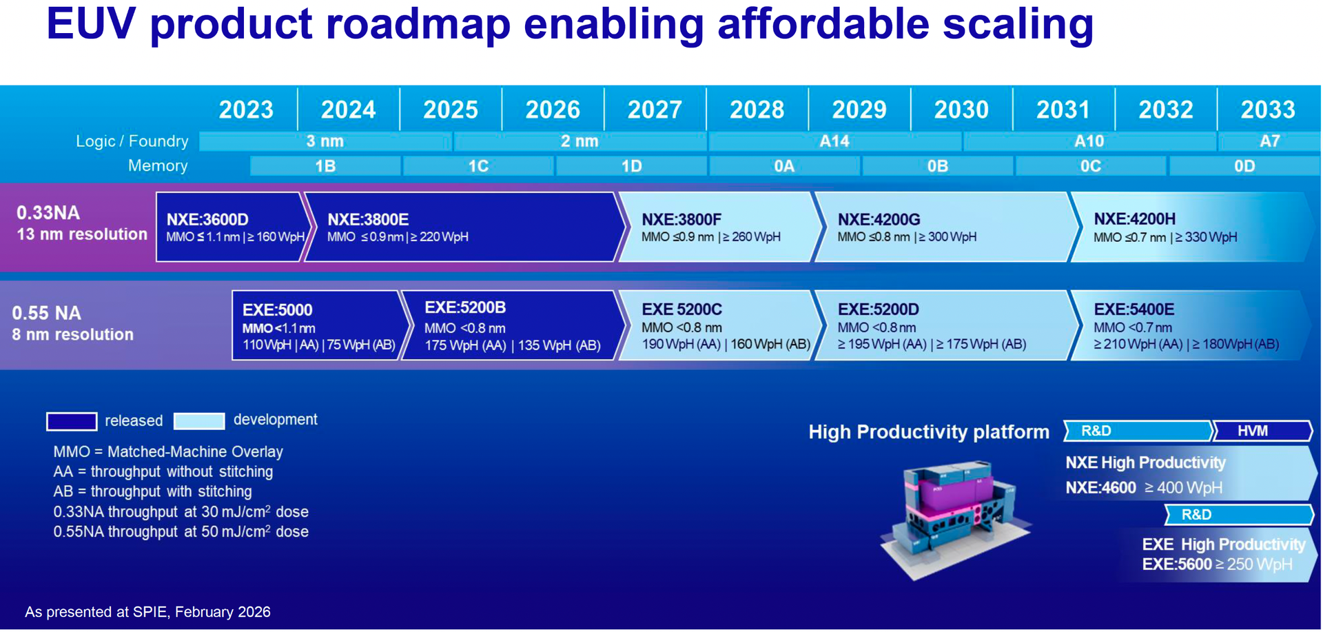
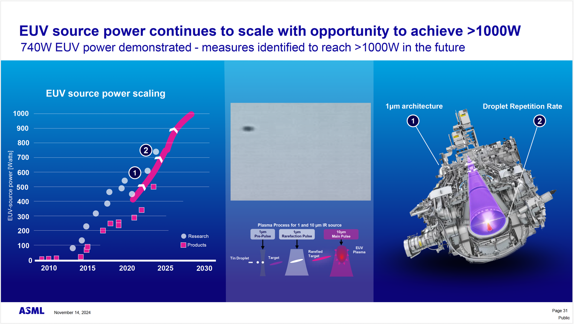
Despite major challenges, ASML has gradually increased the source power of its LPP light sources from around 250W to around 500W and plans to increase it to 1000W in the coming years. In addition, the company plans to almost double the number of generated tin droplets to 100,000 every second.

ASML

(Image credit: ASML)

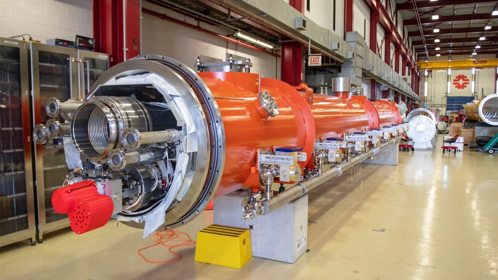
A free-electron laser (FEL) generates EUV light by accelerating electrons to nearly the speed of light and passing the electron beam through an undulator, a series of alternating magnets that force electrons to oscillate and emit radiation. Interaction between the electrons and their radiation causes them to form microscopic bunches and emit light with a 13.5-nm wavelength. This approach eliminates tin droplets and associated debris (that require usage of protective pellicles on photomasks) as well as potentially provides substantially higher EUV power than LPP sources. Furthermore, one FEL can potentially replace multiple LPP sources with a single FEL and a large EUV beam-distribution system.

Yet, there is a major tradeoff: instead of a relatively compact LPP, FEL requires a highly complex particle accelerator, an electron source, a long undulator, electron-beam control, radiation shielding, and an extremely complex distribution system featuring mirrors capable of handling and distributing very high EUV power without losing too much of it along the way. The whole machine must achieve semiconductor fab levels of availability, efficiency, and cost, something that took ASML and the rest of the industry years to achieve.

xLight

(Image credit: xLight)

So, while there is a great enthusiasm surrounding FEL in China, the U.S., and Japan, it will likely take a decade, if not more, before FEL will be able to rival LPP in real semiconductor production facilities. The technology will likely devour billions of dollars in the meantime, so not all entities currently pursuing FEL will live that long.

  •  

Huawei details AI accelerator roadmap, pulls in next-generation Ascend NPUs by several quarters — FP4 performance of the Ascend 960PR doubles expectations

Huawei has updated its AI hardware roadmap by adding new accelerators and supporting processors and pulling in next-generation Ascend 960 accelerators at its annual Huawei Connect event. Specifically, the company accelerated its Ascend 960 roadmap, disclosed Ascend 970 and 980 specifications, introduced its Peerium architecture based on the UnifiedBus, and expanded its vertically integrated AI infrastructure portfolio.

Huawei is currently in the middle of transitioning from its SIMD architectures that it has used for almost a decade with its Ascend accelerators (or neural processing units, how the company prefers to call them) to its all-new SIMD+SIMT architectures that bring together vector-based processing and thread-level parallelism to improve hardware utilization and performance across a variety of AI workloads (SIMD for data parallel operations and SIMT for branch-heavy workloads).

Huawei Ascend AI chip

Image is for illustrative purposes only. (Image credit: Huawei)

The first Ascend NPUs to adopt Huawei's new architecture are Ascend 950PR for prefill and recommendation, as well as Ascend 950DT for decoding and training. Huawei said at the event that its Ascend 950 platform is gaining traction as the Atlas 950 SuperPoD systems are already in large-scale commercial use, though it did not elaborate. The company said tests of its training-oriented Ascend 950DT have produced 'good results' and expects numerous Chinese AI developers to begin training models on 950DT-based systems next year. Meanwhile, Huawei acknowledged that its production capacity remains insufficient to satisfy domestic demand.

Indeed, in September 2025, Huawei announced the maximum Atlas 950 SuperPoD configuration as 2,048 Kungpeng 950 CPUs, 8,192 Ascend 950DT NPUs, 160 cabinets (128 compute + 32 communications), 8 FP8 EFLOPS, 16 FP4 EFLOPS, and 16 PB/s of aggregate interconnect bandwidth. However, in July 2026 Huawei publicly showed a real Atlas 950 SuperPoD implementation with 256 CPUs as well as 1,024 accelerator cards, which is well below the maximum configuration. While the company still describes the architecture as scaling up to 8,192 NPUs, it is not listed on its website, so we can only wonder which systems are now in large-scale commercial use.

For now, the adoption of the Atlas 950 SuperPod does not seem to be proceeding rapidly, perhaps because of insufficient supply, or maybe because of the all-new architecture that requires major redesign of software. In any case, the Atlas 950 SuperPod will in many ways be a pipecleaner for the company to clear the road for more capable Ascend 960-series accelerators and their successors.

Speaking of the Ascend 960, this family will start with the Ascend 960DT in Q1 2027, when it is set to be formally available, three quarters earlier than previously planned.

Huawei Ascend

(Image credit: Huawei)

The Ascend 960DT accelerator is expected to deliver 2 FP8 PFLOPS and 4 FP4 PFLOPS, carries 288 GB of presumably HiZQ memory with 9.6 TB/s bandwidth, and features a 2.2-TB/s interconnect.

The Ascend 960PR NPU follows in Q3 2027, one quarter earlier than originally planned, with 2 FP8 PFLOPS for training, but 8 FP4 PFLOPS for inference (2X higher than Huawei announced last year). The unit carries 192 GB of memory providing 2.4 TB/s of bandwidth and retains the 2.2-TB/s interconnect. For comparison: Nvidia's VR200 GPU due in Q4 2026 can deliver 35 NVFP4 PFLOPS for training and 50 NVFP4 PFLOPS for inference while carrying 288 GB of HBM4 memory.

"We are evolving our Ascend chip series on a one-generation-a-year cycle," said David Wang, the Deputy Chairman of the Board and Rotating Chairman at Huawei, in his keynote. "In 2028 and 2029, we will roll out the Ascend 970 and 980 chips, respectively. Thanks to the Tau (τ) Scaling Law, not only will their compute specifications continue to double, but you can also expect to see huge improvements across the board in terms of memory bandwidth, memory capacity, interconnect bandwidth, and more."

Huawei Ascend roadmap

NPU

Targeted Release

Architecture

FP8 Performance

FP4 Perf

Memory

Memory Bandwidth

Interconnect Bandwidth

Supported Formats

Ascend 910C

2025 Q1

SIMD

–

–

128 GB

3.2 TB/s

784 GB/s

FP32, HF32, FP16, BF16, INT8

Ascend 950PR

2026 Q1

SIMD + SIMT

1 PFLOPS

2 PFLOPS

128 GB of HiBL 1.0

1.6 TB/s

2.0 TB/s

FP32, HF32, FP16, BF16, FP8, MXFP8, HiF8, MXFP4

Ascend 950DT

2026 Q4

SIMD + SIMT

1 PFLOPS

2 PFLOPS

144 GB of HiZQ 2.0

4.0 TB/s

2.0 TB/s

FP32, HF32, FP16, BF16, FP8, MXFP8, HiF8, MXFP4

Ascend 960DT

2027 Q1

SIMD + SIMT

2 PFLOPS

4 PFLOPS

288 GB

9.6 TB/s

2.2 TB/s

FP32, HF32, FP16, BF16, FP8, MXFP8, HiF8, MXFP4, HiF4

Ascend 960PR

2027 Q3

SIMD + SIMT

2 PFLOPS

8 PFLOPS

192 GB

2.4 TB/s

2.2 TB/s

FP32, HF32, FP16, BF16, FP8, MXFP8, HiF8, MXFP4, HiF4

Ascend 970

2028

SIMD + SIMT

3.6 PFLOPS

14 PFLOPS

288 GB

14.4 TB/s

4.4 TB/s

FP32, HF32, FP16, BF16, FP8, MXFP8, HiF8, MXFP4, HiF4

Ascend 980

2029

SIMD + SIMT

7.2 PFLOPS*

28 PFLOPS*

384 GB

38.4 TB/s*

8 TB/s*

FP32, HF32, FP16, BF16, FP8, MXFP8, HiF8, MXFP4, HiF4*

Starting with the Ascend 960-series and onwards, Huawei plans to maintain a one-generation-per-year cadence for its AI accelerators. Pulling in the Ascend 960DT by several quarters is, without any doubt, a remarkable achievement. However, what is even more extraordinary is that Huawei has managed to increase FP4 performance of the Ascend 960PR by two times compared to original expectations, which likely means that the company has substantially reworked the processor's low-precision compute capabilities rather than merely adjusted its memory subsystem or clock speeds. In fact, four-fold higher FP4 performance compared to FP8 is set to be a distinctive feature of Ascend 970 and 980.

The Ascend 970 is due in 2028 with 3.6 FP8 PFLOPS, 14 FP4 PFLOPS, 288 GB of memory providing 14.4 TB/s, and 4.4 TB/s of interconnect bandwidth. Ascend 980 follows in 2029 with 7.2 FP8 PFLOPS and 28 FP4 PFLOPS, along with 384 GB of memory reaching 38.4 TB/s and an 8-TB/s interconnect. Huawei marks the Ascend 980 figures as preliminary.

  •  

Apple eyes Nvidia NVLink to power its new custom M8 Ultra AI servers — historically bitter rivals reportedly team up for 2029 data center push

Apple is reportedly developing AI servers based on its own M-series processors and is evaluating NVLink Fusion technology for interconnects, according to The Information. The machines are expected to use M8 Ultra processors and arrive in 2029, the report claims. For now, the usage of the NVLink Fusion platform is not formalized and has not been confirmed by either Apple or Nvidia, but if Apple decides to use it instead of competing solutions, this may have significantly broader market implications than just Apple using Nvidia hardware.

Apple looking for fast interconnects

Apple is reportedly considering at least two server configurations: a smaller machine equipped with two M8 Ultra processors and a higher-end version featuring four M8 Ultra system-on-chips. Although Apple has its own UltraFusion technology for stitching two high-end SoCs together seamlessly, it looks like the company does not have a proper solution for scale-up and scale-out connectivity of its processors, which is where Nvidia's NVLink Fusion comes into play. Apparently, Apple wants to use NVLink infrastructure, which includes not only an interconnection protocol, but also switches, chiplets that add NVLink connectivity, and a software stack, for its servers. The project was reportedly initiated around a year ago and was backed by John Ternus while he headed Apple's hardware engineering organization.

Apple already builds custom servers for Private Cloud Compute, which handle AI workloads too demanding for local execution on iPhones and Macs, The Information claims. Most of these machines use Apple's internally developed connectivity technologies, which are reportedly too slow and costly for large-scale commercial deployments, which is why Apple is looking elsewhere.

More than NVLink?

The Information specifically mentions Apple's need for connectivity technology suitable for large-scale deployments, although it does not explain exactly what this means architecturally. If the publication is referring to connecting multiple servers into larger clusters, this would normally be the job of scale-out technologies such as Ethernet or InfiniBand, rather than a scale-up fabric such as NVLink. Nvidia originally developed its NVLink fabric technology to scale-up performance of its accelerators, so the technology is optimized for accelerator-to-accelerator connectivity and enables a rack of Nvidia GPUs to function as a tightly coupled compute domain. There is a different implementation called NVLink-C2C, which is a coherent chip-to-chip interface for connecting CPUs to accelerators and CPUs to CPUs

Meanwhile, modern Apple M Pro and M Ultra processors are system-in-packages consisting of a CPU chiplet and a GPU/neural engine chiplet, which are stitched together using TSMC's SoIC-mH technology. If Apple continues to use this architecture (very likely), an M8 Ultra processor can be considered as a CPU and an accelerator. However, this raises the question of how Apple intends to connect M8 Ultra processors to NVLink and which components of the SiP would participate in the NVLink domain. One possibility is that Apple could expose the accelerator portion of M8 Ultra to NVLink through an NVLink Fusion chiplet, which effectively means it will treat it as an accelerator for a scale-up domain. Another possibility is that Apple is developing a different accelerator architecture for its servers, perhaps by simply placing the GPU/NPU chiplet onto a separate substrate/interposer and equipping it with its own memory, though there is currently no evidence that confirms such a design for a chip that is years away.

Another thing to keep in mind is that Apple is a member of the UALink Consortium, an organization overseeing development of industry-standard UALink accelerator-to-accelerator interconnections that supports up to 1,024 accelerators. While for now there is a limited choice of UALink switches, by 2029, there will be industry-standard switches offering different performance and capabilities, which makes the choice of NVLink as a scale-up fabric even stranger.

One possible explanation is that Apple is interested in considerably more than NVLink itself. NVLink Fusion is part of Nvidia's rack-scale and data center infrastructure architecture, which can combine NVLink scale-up connectivity with Nvidia's Spectrum-X Ethernet or Quantum-X InfiniBand scale-out networks, including switches equipped with co-packaged optics. Thus, Apple could potentially adopt Nvidia technology for both scale-up and scale-out connectivity instead of developing an entire data center networking stack of its own. This is merely speculation for now, but such an approach would effectively mean that Apple is building AI servers around significant portions of Nvidia's data center architecture while retaining its own processors and not using Nvidia accelerators. If this happens, this will be a testament that Nvidia is now setting de facto standards for AI data centers, no matter which AI accelerators and CPUs are used.

Burying the hatchet?

Without a doubt, Nvidia is a leading supplier of data center hardware, so it is logical for Apple to work with the company if the two companies are indeed working together on Apple's data center platform.

Apple and Nvidia are not exactly good partners. The feud between the two companies began in the early 2000s, when Steve Jobs accused Nvidia of infringing on Pixar's patents on which Nvidia responded that it owned more graphics IP than Pixar and therefore could sue the company. Later on, Apple and Nvidia had disagreements over GPU design decisions that the latter supplied to the former. However, then came 'Bumpgate' as Nvidia supplied Apple and other PC makers defective GPUs in 2007 – 2008, did not acknowledge the problem, and then resisted fully compensating Apple and other PC makers for their repair costs, which is when the relationship between the companies got especially dire. Apple continued to use Nvidia GPUs till 2014 or 2015, at which point it switched to AMD's Radeon, and then abandoned discrete third-party GPUs altogether.

More recently, Apple started to use Nvidia's hardware again. The latest Siri AI is primarily powered by Apple Foundation Models developed in collaboration with Google using Gemini technology. Server-side inference runs through Apple's Private Cloud Compute architecture, and many of the workloads are hosted on Nvidia Blackwell GPUs in Google Cloud. Yet, using Nvidia hardware in the cloud and adopting the company's technologies for your own platforms is a completely different thing.

  •  

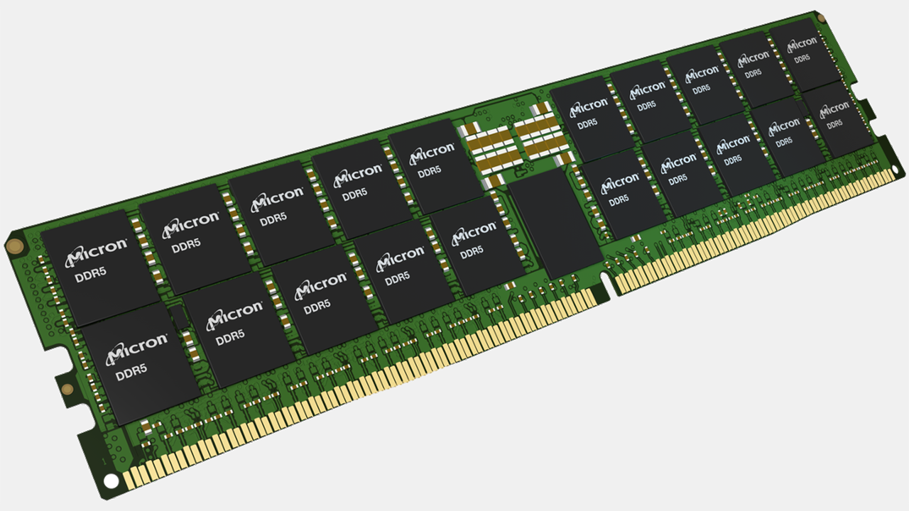
Micron announces 512GB DDR5-9200 memory modules with 16W power draw — up to 12TB per server, claims 60% less energy-intensive than four 128GB modules

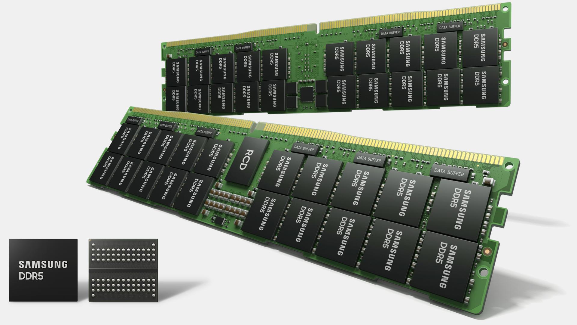
Micron this week introduced its first 512GB DDR5-9200 memory module that is designed for servers used for applications that demand a lot of memory. The new modules — which are currently being validated by AMD and Intel with their next-generation server platforms — will enable server makers to build machines with up to 12TB of fast memory. What remains to be seen is the price of such modules and servers.

To build its 512GB DDR5 RDIMM, Micron uses advanced packaging that stacks multiple DRAM dies vertically and connects them using through-silicon vias (TSVs). The company does not disclose which memory devices and how many of them it uses, but claims that a single 512GB RDIMM consumes over 60% less operating power than four 128GB modules — based on 16.0W for one 512GB module compared with the 44.2W total for four 128GB modules — which suggests that we are dealing with fairly advanced ICs.

Micron's 512GB module is not the industry's first 512GB DDR5 RDIMM — that achievement belongs to Samsung — but it is certainly the industry's first 512GB module certified to operate with a 9200 MT/s data transfer rate with standard 1.1V voltage (which implies on usage of Micron's 16Gb DDR5-9200 devices made on its 1γ (1-gamma) fabrication process that uses EUV lithography and consumes 20% less power than predecessors, though we are speculating).

Truth to be told, 512GB DDR5 memory modules are rather niche products, which is perhaps why Samsung's 512GB RDIMMs formally introduced in 2021 have not become widespread even after AMD and Intel introduced processors with over 100 cores. Micron positions its 512GB DDR5 RDIMM primarily for servers running analytics, in-memory databases, simulations, virtualization, agentic AI, and other workloads demanding high-core-count processors and plenty of memory. As processors with 200 or more cores emerge, 512GB modules may become more relevant as 12TB of memory in a server running two 256-core CPUs means 24GB per core, which no longer looks particularly excessive for applications like in-memory databases, analytics, or caching.

Micron claims that in memory-constrained Spark Support Vector Machine (SVM) analytics workloads, systems featuring 512GB memory modules can provide up to 1.4 times the performance of configurations equipped with 256GB DDR5 modules, though the company does not disclose how much memory in total these systems use. Micron also says the higher-capacity memory can increase throughput and concurrency for memory-intensive database and caching applications such as RocksDB and Redis.

AMD and Intel are working with Micron to qualify the new modules for their upcoming server platforms. Micron plans to begin volume production of its 512GB DDR5 RDIMMs sometime in the second half of 2027 and intends to align the schedule with customer requirements.

One of the more pressing questions about Micron's 512GB DDR5-9200 memory modules is their price. A 256GB DDR5-6400 RDIMM currently retails for around $19,000. Given the unique proposition that 512GB modules have for memory-constrained applications, such modules can cost significantly more than 256GB memory sticks, which will not help their broad adoption.

  •  

Jensen Huang thinks China will develop its own advanced lithography chipmaking tools by 2030 — Nvidia CEO says achievement of that capability 'is just a matter of time'

China's progress toward technological self-sufficiency in recent years is undeniable, but there is one thing that the country has so far failed to develop: lithography tools that are on par with those offered by ASML. That shortcoming has greatly hampered its domestic semiconductor industry. But Nvidia CEO Jensen Huang believes China will develop its own advanced lithography systems in just three or four years.

"They are going to get there by 2030," Huang said in an interview with The All-In Podcast (at 43:43). "2030 is just around the corner. The way to think about China is that it is really good at high-volume production. It is just a matter of time[...] so two or three years is just a click; it is nothing. So as far as they are concerned, they are already there."

Huang tends to look optimistically at China's technological development. Specifically, he is known for calling China's AI industry as being 'right behind' American frontier labs, which may well be correct, given how much capital China is investing in AI. But when it comes to the Chinese semiconductor industry in general and its lithography sector in particular, Huang may be too optimistic.

At present, China's leading producer of lithography tools — Shanghai Micro Electronics Equipment — can mass-produce a 193-nm ArF dry scanner that can be used to build chips on 90nm-class process technology. While the company has reportedly developed a 28nm-capable ArF immersion scanner, there is no public evidence that such systems are produced in volume and are used for high-volume chip production.

Although there are reports that Shanghai Aishengna Electronic Technology Group (a unit, or an affiliate of SMEE) has delivered its first immersion scanner that may be capable of printing chips using 28nm-class process technology, these tools will require extensive qualification before they can be used for high-volume manufacturing of semiconductors, so if deployment follows standard timelines, it will take years before this unit will be used for mass producing chips.

Even assuming that the first scanners are delivered to Chinese chipmakers in 2026, widespread production use before 2028–2029 appears unlikely. Furthermore, matching the capabilities of an early-generation ASML immersion scanner would still leave Chinese lithography suppliers considerably behind ASML's contemporary systems, which makes technological parity in ArF immersion lithography by 2030 highly unlikely.

China is considerably further behind in extreme ultraviolet (EUV) lithography. While there are reports that Chinese scientists have managed to develop a laser-produced plasma source that can generate the 13.5-nanometer wavelength light required for the technology, it does not look like China is close to assembling even a prototype EUV scanner itself.

Even if China can assemble an EUV experimental exposure platform without having mastered production-quality immersion DUV, it is hard to imagine a Chinese company producing EUV scanners without solving the hardest problems common to both DUV and EUV technologies. A production lithography scanner requires extraordinary capabilities in wafer and reticle stages, alignment, overlay, projection optics, and metrology, just to name a few.

If China is still struggling to industrialize these capabilities for immersion DUV, there is little reason to assume it has somehow solved them at the substantially more demanding EUV level. But given the potentially existential stakes of the AI race, and the determination of the Chinese government to achieve technological self-sufficiency, it may just indeed be a matter of time.

  •  

Russian freelancers use Claude to program autonomous combat drone swarm — AI-enabled target selection and detonation without a human in the loop

Hit hard by sanctions and lacking resources, Russia is left to rely on foreign advanced technologies to compensate. Russia-linked agents appear to use Claude for a broad range of activities, from propaganda and espionage to the procurement of military/dual-use equipment and the development of autonomous drone swarms, according to Anthropic's September 2026 threat report.

Anthropic identified a small team of Russia-based freelance developers who used Claude to build software for an autonomous combat-drone swarm called DronDoc or Serafim. Claude helped develop swarm coordination, computer vision, terminal guidance, and other software that enabled drones to select targets—including people—and issue detonation commands without a human in the loop. The developers trained their computer-vision system on Ukrainian combat footage and used locations in Ukraine for simulated missions. Meanwhile, they loaded software onto real development boards for hardware-in-the-loop testing, though it is unclear whether they field-tested it.

The developers used Claude Code extensively to build and test the swarm software, and they circumvented Anthropic's geographic restrictions by routing traffic through commercial VPNs. Once Anthropic identified the activity as suspected weapons development, it banned the accounts associated with the group and incorporated what it learned into additional safeguards. Meanwhile, the key distinction is that the safeguards did not stop the project immediately, and based on the disclosure, Claude Code clearly helped advance the autonomous drone swarm program.

Anthropic gathered enough information about the people/accounts and their activity to assess what kind of group they were, so it claims that they were not a Russian state entity. Meanwhile, although Anthropic likely identified the company or organization, it did not publicly name it.

In addition, Anthropic discovered a Russian state-linked cyberespionage operation that used Claude to automate everything from infrastructure setup and phishing to malware development and data exfiltration. The campaign targeted more than 20 organizations, including Ukrainian and European government, military, intelligence, and defense entities.

Last but not least, Russia-linked actors also used Claude for propaganda operations, including a Russian state-directed campaign in the Central African Republic that produced pro-Russian and pro-Wagner content for radio, local media, and Telegram.

Most alarming, the report shows AI is now doing work that previously required teams of software engineers, intelligence analysts, and security specialists. While Anthropic's safeguards block many malicious requests, the company admits they cannot block all of them.

'Biological misuse of AI'

Anthropic admits that 'biological misuse' — a term that it uses to soften activities involving biological weapons, dangerous pathogens, poisons, and toxins — is one of the most serious risks of frontier AI models. While older models such as Claude Opus 4 and Sonnet 4.5 were demonstrably below the threshold for meaningfully assisting sophisticated biological research, Anthropic can no longer make the same assurance about today's models.

In its report, Anthropic identified five cases in which researchers, some associated with state-backed programs and military institutions, used Claude for biological research that could potentially assist biological-weapons development. Anthropic does not identify the countries, organizations, or individual researchers behind its five biological-misuse case studies. Furthermore, it deliberately withholds these details, so the report does not attribute any of them to China, Iran, Russia, or any other specific country. Furthermore, it does not outright allege that researchers are building bioweapons.

  •  

Anthropic CEO warns of AI-driven botnet 'swarm' taking over the entire internet — 'In 6–12 months such a swarm could be capable of taking over the entire internet with a persistent botnet'

The progress of artificial intelligence technologies in recent years is undeniable, and its pace is pretty much unbelievable. With at least four American contenders with frontier AI models, the competition is intense, and the development of new models is moving fast. Yet, Dario Amodei, chief executive of Anthropic, has called for slowing down the development of new AI models, even warning of a potential AI-powered botnet swarm that could take over the entire internet.

"Given the accelerating rate of AI capability development, it is my worry that in 6–12 months such a swarm could be capable of taking over the entire internet with a persistent botnet (potentially causing hundreds of billions of dollars in damage), and that the scale of damage would continue to increase from there if AI becomes more powerful without the necessary guardrails," Dario Amodei, chief executive of Anthropic, wrote in an open letter.

Dario Amodei's vision is to a large degree shared by Evan Hubinger, an AI scientist who exited Anthropic recently, who then said there was a 10% chance humanity was set for extinction by the end of the decade. "We really do earnestly believe AI could kill all humans," Hubinger wrote in an X post. "I personally think it is >10% within the next decade. I believe Anthropic is trying its best, but we do not yet have a plan to solve alignment for superintelligence and are not clearly on track to."

In universes created by James Cameron (Terminator) and Frank Herbert (Dune), AI is posed as a dangerous invention. But let us take a closer look. Further development of AI is moving from answering questions to autonomously performing complex multi-step tasks, something that previously required teams of skilled human specialists, which turns us to how adversaries use Anthropic's AI capabilities, lacking human resources.

Anthropic's own findings show that today's AI models can already assist with weapons engineering, military intelligence, surveillance, cyber operations, and other potentially destructive activities, while more capable successors could dramatically reduce the expertise, manpower, and time required to conduct them.

The findings echo two rather different warnings from science fiction: James Cameron's Terminator showed the consequences of losing control over autonomous military AI, whereas Frank Herbert’s Dune imagined humanity eventually outlawing AI after becoming dangerously dependent on them.

Meanwhile, greater capability does not automatically translate into greater danger. For example, more advanced AI technology can also have stronger safeguards, detect malicious activity, and automate work that so far has not been automated.

Halting AI development could also be counterproductive if less responsible companies or countries continue advancing their models. In fact, leaving the most capable AI systems in the hands of actors that are known for military aggression is no less dangerous than leaving a monkey with a grenade.

  •