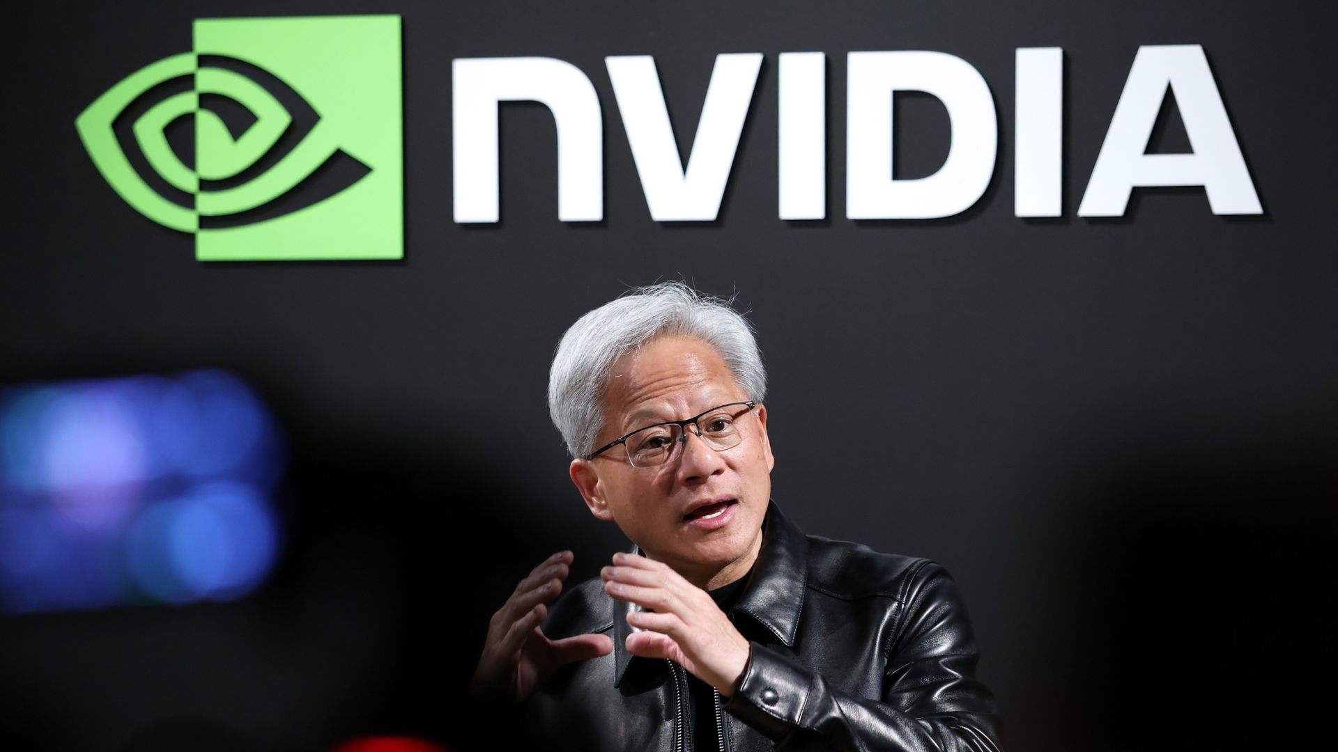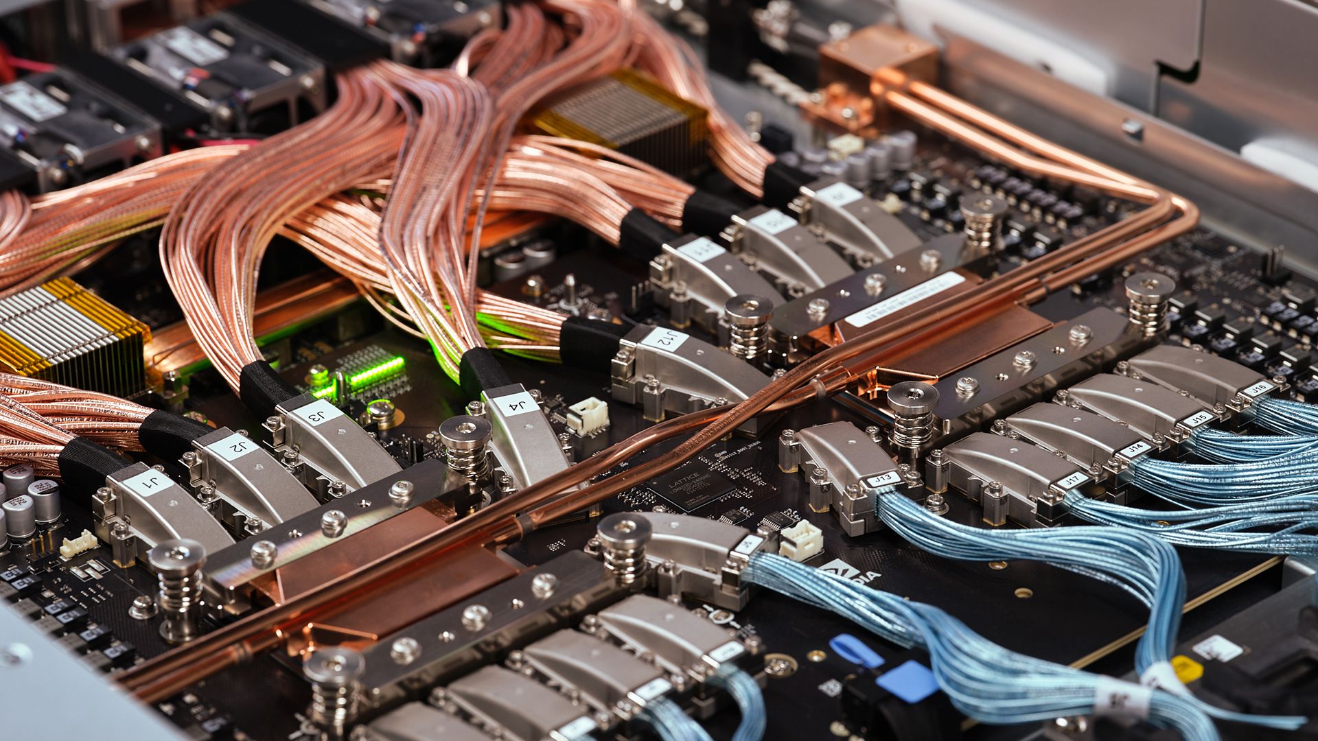
Nvidia’s $5 billion purchase of Intel stock last year, made as part of the companies’ strategic AI infrastructure partnership announced in September, has become a highly lucrative investment, generating nearly $25 billion, the company revealed in an SEC filing this week. In addition, Nvidia owns nearly $21 billion worth of SpaceX stock and holds stakes valued at more than $10 billion in various customers, partners, and suppliers.
With quarterly revenue exceeding $80 billion and net income approaching $60 billion, Nvidia has plenty of unspent cash to invest. Traditionally, the company tends to invest in stocks poised to grow, as well as make strategic investments.
Without a doubt, Nvidia's investment in Intel was both strategic and financial, as it helped Intel survive hard times and has generated $24.989 billion for the company. Interestingly, after investing in Intel, Nvidia has sold its 1.1 million Arm shares (worth $178.1 million last August). Without any doubts, Nvidia will continue developing Arm-based CPUs, though for now it does not own any Arm stock.
The SpaceX investment — valued at $20.975 billion — seems entirely strategic at present, since SpaceX's xAI has committed to exclusively using Nvidia hardware in its AI data centers both on Earth and in orbit. Once SpaceX's stock regains its lost value, Nvidia may well earn on it, though it remains to be seen when this happens.
Other notable investments that Nvidia has made over the past year include Coherent, a major maker of lasers, optical materials, and semiconductors; Nokia, a telecommunications giant; and Synopsys, an electronic design automation (EDA) provider.
Coherent is expected to make Ultra-High-Power Continuous-Wave (UHP CW) lasers for Nvidia's next-generation data center platforms relying on co-packaged optical (CPO) interconnects, so Nvidia invested $2 billion in the company earlier this year. Since then, the stock has almost skyrocketed.
Something similar happened to the Nokia investment. Last October, the company announced plans to invest $1 billion in Nokia to accelerate AI-RAN innovation and lead the transition from 5G to 6G. By now, the shares that Nvidia owns are worth $2.2 billion.
Synopsys has been aggressively adding artificial intelligence capabilities for its tools, so to support the company, Nvidia acquired $2 billion worth of Synopsys stock last December. Right now, the stake is valued at $2.15 billion, making it a profitable investment for the AI hardware giant.
In addition, Nvidia continues to own stock of its clients, but the picture is different for CoreWeave and Nebius. Last year, the company owned 24.277 million CoreWeave shares worth $3.959 billion. Nvidia now owns 47.213 million shares of CoreWeave valued at $4.699 billion, which essentially means that the company substantially increased its position as CoreWeave's stock price declined. As for Nebius, Nvidia's position remained at 1.19 million shares, but while the stake was worth $65.869 million in 2025, its value has since surged nearly fivefold to $328.77 million.
What could possibly go wrong when you try to steal trade secrets from a restricted facility using a 360-degree action camera hidden in snacks? Forgetting to turn off the device’s Bluetooth and Wi-Fi transmitters, as it turns out.
A senior engineer at Nanya Technology has been indicted in Taiwan for allegedly copying 32 files containing information about the company's DRAM manufacturing process, reportsFreedom Times. The engineer was reportedly in talks with Chinese recruitment agencies and allegedly planned to pass Nanya's trade secrets to its next employer in the People's Republic in exchange for higher compensation.
Yeh Yen-wei, a senior engineer in the Advanced Process Development Division at Nanya, joined the company in 2022 and began to communicate with Chinese recruiters in 2025 to explore employment opportunities in the People's Republic. Sometime in mid-February 2026, he submitted his resignation. However, before leaving the company in mid-April, on March 28, April 4, and April 5 — during weekends and either late at night or early in the morning — he visited the company's restricted office areas with his Insta360 X4 Air action camera hidden among snacks to get it past security checks.
Once inside, Yeh used his legitimate account credentials to access Nanya's virtual machines and opened various internal research and development documents. He then used the camera to capture photographs and video of information associated with Nanya's DRAM process technologies and production methods. It goes without saying that he retained the information when he officially resigned from Nanya in mid-April.
However, his actions did not go unnoticed. Nanya's IT security team detected 'abnormal' wireless signals inside the company's restricted facilities (i.e., identified the device using its Bluetooth and/or Wi-Fi signals) and tied them to the employee's access records and activity logs. Eventually, Nanya reported the suspected theft to Taiwanese authorities, which led to an indictment.
The New Taipei District Prosecutors Office charged Yeh under Taiwan's Trade Secrets Act with unauthorized reproduction of trade secrets intended for use in China, an offense for which he faces up to 10 years in prison, as well as with breach of trust under the Criminal Code. Meanwhile, forensic examination of the seized equipment uncovered no evidence that Yeh had successfully transmitted Nanya's confidential information to a Chinese company or anyone outside the company, so he could potentially get off easy.
Russia's latest S-71 'Monochrome' cruise missiles use Nvidia's Jetson Orin modules with artificial intelligence capabilities, the Main Directorate of Intelligence of the Ministry of Defense of Ukraine claimed on Wednesday. The S-71 'Monochrome' is distinguished by reduced observability and autonomous targeting capability, reports Militarnyi. Nvidia says the Jetson Orin is a consumer-grade device that is not export-controlled and is not officially available in Russia.
According to the claims, the module in question carries an Nvidia chip marked as SNVUP6.MOP TE980M-A1 and resembles the Jetson Orin NX 8GB/16GB system-on-module. The Orin NX is an automotive-grade SoM based on a system-on-chip featuring up to eight Arm Cortex-A78AE cores, a GPU featuring Ampere architecture with 1024 CUDA cores and 32 Tensor cores that provide up to 157 sparse INT8 TOPS performance for AI, dedicated NVDLA engines, and a vision accelerator. The unit has been shipping since 2023, though based on the markings on the chip purportedly found in the missile, it was packaged in March, 2025.
"Our Jetson Orin modules are consumer-grade products sold to students, developers, and startups for a wide range of beneficial applications," an Nvidia spokesperson told Tom's Hardware. "They are not available in Russia and are not designed for military purposes. Pre-owned Jetsons are available through many reseller channels. Although we cannot track products after they are sold, if we determine that any customer is violating U.S. export controls, we will take appropriate action."
Nvidia positions Jetson Orin NX as a solution for space- and power-constrained applications that need vision, but cannot accommodate more powerful and power-hungry solutions, which essentially means drones and mobile robots that work on battery power. Conceptually, an Orin NX could function as a dedicated electro-optical perception computer that can recognize images locally and pass the information to a separate flight-control/guidance system.
In the S-71 'Monochrome' missile, capabilities of Nvidia's Jetson Orin NX are potentially useful as the compute engine behind an electro-optical perception system (based on a Honpho TS130C-01 module that is made in China) that recognizes images in real time and assists terminal guidance. As per Militarnyi, the S-71M 'Monochrome' can be fired from Su-57 fighters or S-70 Okhotnik drones. With a range of up to 300km, it carries a 250k high-explosive fragmentation bomb as its payload.
Nvidia's Jetson Orin NX modules have been shipping since 2023 and are widely available, which means that Nvidia sells hundreds of thousands, if not millions, every year. Meanwhile, the majority of Jetson Orin NX-based products available in retail are not the SoMs themselves, but rather small-form-factor systems or development kits. The modules are available too, though not as widely. For example, a German store sells them for €685 with a 19% VAT.
In any case, while the American government does export control for high-end AI accelerators like Nvidia's H100 or B200, which can be used to train AI models that can later be used for military purposes, it does not export control hardware that can run these models locally. Ultimately, the models are trained anyway, and the hardware that can use them is readily available.
Coming on the heels of Intel's $19.7 billion common stock offering from earlier this week, AMD on Thursday announced plans to borrow $4.75 billion through a new senior unsecured debt offering. AMD does not tie the proceeds to a particular project, saying they will be available for general corporate purposes, including potentially paying down existing debt. Meanwhile, the increasing capital intensity of the industry gives AMD numerous options to use the money.
"We intend to use the net proceeds from this offering for general corporate purposes, which may include the repayment of debt," an AMD statement with the Securities and Exchange Commission reads.
The offering comprises four tranches: $1.25 billion of 4.6% notes due in 2029; $1.50 billion of 5% notes due in 2031; $1 billion of 5.25% notes due in 2033; and $1 billion of 5.5% notes due in 2036. Their yields to maturity are 4.64%, 5.018%, 5.264%, and 5.532%, respectively, while spreads over comparable U.S. Treasuries range from 43 to 90 basis points, which indicates that the market is generally confident in AMD and is willing to lend it money at rates that barely exceed those of the U.S. Treasury. Moody's and S&P are expected to rate the securities A1 and A, respectively.
AMD did not disclose how it plans to spend $4.75 billion, but the additional money obtained at attractive rates gives it room to finance its increasingly capital-intensive business as well as cash for debt repayment and other corporate requirements.
AMD hardly appears desperate for additional money. At the end of Q2 2026, the company had approximately $13.1 billion in cash, cash equivalents, and short-term investments. AMD's debt totaled $3.2 billion, and only $875 million is classified as current, which means that the proceeds from the offering by far exceed AMD's current obligations. Meanwhile, AMD's business is becoming very capital intensive.
At the end of 2025, the company had around $12.2 billion in unconditional commitments, which include purchases of wafers and substrates, multi-year cloud-service agreements, software and technology licenses, and guaranteed obligations to third parties. Approximately $8.5 billion was due in 2026.
Also, AMD's working capital requirements are growing. Inventories reached approximately $8.47 billion by the end of Q2, while accounts payable climbed to $5.36 billion. AMD also spent $1.20 billion on property and equipment during the first half of 2026, compared with $494 million a year earlier.
If we were to speculate where AMD can put $4.75 billion, then long-term supply agreements for commodities like memory, logic production, or advanced packaging immediately come to mind. However, given the current market realities, $4.75 billion is 1.8x smaller than AMD's inventories as of late Q2 2026. Furthermore, an average long-term supply deal with a major memory maker now amounts to $7.14 billion (according to Micron's comments made in its recent earnings release).
That said, $4.75 billion may not be enough for AMD to make strategically important purchase commitments. Nonetheless, getting nearly $5 billion at attractive rates amid global undersupply of pretty much everything certainly gives AMD some additional flexibility to run its business.
Intel chief executive Lip-Bu Tan has invested $12 million of his own money in Intel this week as part of the company's $19.7 billion stock offering, indicating his confidence in the company. Meanwhile, Bank of America analysts view the capital raise as an indicator of management's 'increasing foundry conviction,' suggesting growing confidence in Intel's foundry prospects.
"The capital raise […] is still a good leading indicator of management's increasing Foundry conviction (vs. defensive balance-sheet action)," reads an excerpt from BofA's note to clients published by John Intel. "We flag the capital raise also aligns with the recent step-up in capex (for internal customer) and ongoing 14A progress, with further capex increase expected on potential incremental external customer wins (18A-P, 14A, advanced packaging EMIB-T)."
Indeed, it is hard to believe that Intel's management would raise almost $20 billion without a more or less clear plan on how to spend it. In fact, Lip-Bu Tan has said repeatedly that he would not authorize building capacity for external customers unless there was a customer commitment. Of course, at some point, Intel will need additional 18A capacity for its own products as well, but $20 billion is a lot of money, which may indicate that the additional capacity will be aimed both at internal and external clients. This is by no means a confirmation that a formal deal has been reached with a big customer like Apple, AMD, Nvidia, or Qualcomm, but it is at least an indicator of management's confidence in Intel's performance going forward.
In fact, Intel's $19.7 billion stock offering was several times oversubscribed and about 33% of investors who submitted orders received no shares at all, reports @FirstSquawk, which indicates great confidence in the company by regular investors. Apparently, Intel's chief executive, Lip-Bu Tan, was among the investors who managed to get $12 million worth of stock using his own money.
"Overall, we view the raise as net positive given foundry scale and customer conviction driving longer term top-line and operational efficiency, more than offsetting modest near-term EPS dilution," the note by BofA reads. "We also flag positive read-through for both front-end and back-end packaging semicap vendors."
Elon Musk told employees of SpaceX that the power capacity of the company's xAI data centers will increase by 7x to 10GW by late 2027. If this happens, the company's data centers will bring the company some $300 billion – $500 billion in revenue per year, according to Musk. The claim comes as SpaceX's market capitalization dropped by nearly $570 billion in less than two months. Meanwhile, the combined performance of the cluster will by far outpace not only all supercomputers in the Top 500, but also all AI clusters running today.
"We have already built the most powerful AI training clusters in the world," Musk told SpaceX employees at a meeting. "What we expect to do by the end of next year is about 10 times more than what we have done thus far. […] So, we are aiming to get to 10 GW [of compute] by the end of next year. […] If the value per watt is probably going to be $30 to $50, which means if we bring 10 GW of AI compute online by the end of next year, it will be $300 to $500 billion a year in revenue. Big numbers."
A lot of power
At present, SpaceX's xAI data centers in Memphis and Southaven have a rated power draw of 1.4 GW. The company plans to increase the electrical capacity of its data centers to 10 GW by the end of 2027, or by around sevenfold in roughly 1.5 years. It should be noted that AI infrastructure with a 'nameplate power draw' of 1.4 GW by far does not offer compute capacity of 1.4 GW.
A large AI data center with a power usage effectiveness (PUE) of roughly 1.2 would have around 1.17 GW available to IT equipment (i.e., 230 MW is used by cooling, pumps, fans, humidification/dehumidification, lighting, power distribution losses, UPS losses, and other facility systems). Not all of that 1.17 GW goes to AI accelerators: CPUs, memory, networking, and storage consume a meaningful share. If perhaps 70% – 80% of IT power ultimately corresponds to accelerators, we might be looking at roughly 0.8 GW – 0.95 GW of accelerator power in the case of a 1.4 GW data center.
Loads of FLOPS
Compute capacity is not measured in Watts; it is measured in floating-point operations per second (FLOPS). Keeping in mind that currently xAI uses a mix of Hopper- and Blackwell-based accelerators, it is hard to determine how much compute xAI has today. Since xAI seems to be betting primarily at Nvidia's Vera Rubin systems from now on, we can make a more or less educated guess about the company's Rubin-based compute capability the company will have by the end of 2027.
Assuming that all of the new 8.6 GW nameplate power draw will be based on Nvidia's NVL72 VR200 rack-scale systems and the PUE of around 1.2, the IT power budget of the new capacity will be 6.88 GW. Actual Rubin AI accelerators will get between 4.816 GW and 5.504 GW of power depending on how much of the IT power will correspond to these GPUs. Each Rubin GPU is expected to consume 2.3 kW of power in Max-P configuration. As a result, xAI's clusters will house between 2.094 million and 2.393 million Rubin GPUs in Max-P mode, or 29,083 and 33,236 NVL72 VR200 systems.
The performance of the NVL72 VR200 system is well known, so depending on the number of these machines that xAI will deploy by the end of 2027, we are looking at rather formidable numbers. NVFP4 inference performance of the cluster will be between 105 and 120 ExaFLOPS; NVFP4 training performance will range from 73 to 84 ExaFLOPS; FP6/FP8 training capability is projected between 37 and 42 EFLOPS, whereas native FP64 compute will total 70 – 80 EFLOPS. Of course, we are dealing with very rough numbers here as some systems may not work in Max-P configuration.
To put the numbers into context. The total combined FP64 performance of all systems on the Top 500 list is 18.73 EFLOPS. xAI will have 3.7X – 4.3X more than that if the cluster is deployed. As for AI performance, 105 – 120 NVFP4 EFLOPS inference and 73 – 84 NVFP4 EFLOPS training put this cluster in a whole different league from anything publicly operating right now, meaning that we are talking about dramatically more sophisticated AI models coming. Whether or not the combined xAI compute capability will enable the company to earn $300 billion – $500 billion per year is something that remains to be seen, as SpaceX is not the only company selling compute capacity to AI companies, and the competition will likely be rough.
Yet, it is about time for Musk to make comments like this, as after topping $2.44 trillion in market capitalization on June 20, SpaceX dropped to $1.43 trillion on August 1, but rebounded to $1.87 trillion on August 12.
Cerebras on Wednesday reported its financial results for the second quarter, and while its earnings nearly doubled year-over-year, its shares plunged more than 18% in after-hours trading as it missed analysts' expectations, Reuters reports. Furthermore, the company's financial results suggest that Cerebras is increasingly succeeding at selling compute delivered by its hardware, rather than the hardware itself.
For the quarter ended June 30, 2026, Cerebras reported revenue of $180.11 million, up from $103.32 million in Q2 2025. Earnings of the company's cloud services totaled $125.99 million, up dramatically from 33.03 million in the same quarter a year ago, but sales of hardware dropped to $54.12 million from $70.3 million in Q2 2025. Wall Street analysts expected Cerebras to earn $194.23 million during the quarter.
During the quarter, Cerebras' operating expenses rose to $502.79 million (up from $89.28 million a year ago), its gross margin dropped to 14%, and it lost roughly $450.53 million. The main reason behind the company's skyrocketing operating expenses and losses is stock-based compensation triggered by its May IPO. Once the IPO happened, the company had to recognize the value of stock-based compensation as its expenses, as stock-based compensation jumped from $13.3 million in Q2 2025 to $377 million in Q2 2025. Without the stock-based compensation, the company's net loss would be $73.53 million.
That said, the analysts were not disappointed by the huge loss, but rather by the earnings miss, the rapidly dropping hardware sales, and uncertain returns generated by Cerebras' new business model.
Missing earnings expectations for an AI hardware company amid the AI market frenzy is not a thing that happens often. But perhaps more importantly is that Cerebras' hardware sales dropped 23% year-over-year, whereas cloud and other services revenue skyrocketed by 281%. On the one hand, this proves that the company's clients are more willing to buy its compute hardware in the cloud rather than own it, which means stable revenue streams. However, Cerebras' new business model requires Cerebras to put enormous amounts of capital into infrastructure before it can earn its cloud revenue.
Under its original hardware model, Cerebras has to manufacture its Wafer Scale Engines at TSMC, assemble systems on its base, and sell its CS systems to customers, which then own the machines, install them in their own or leased data centers, and assume the cost of operating the infrastructure. Under its new model, Cerebras retains and deploys the hardware itself, secures data-center capacity and power, and operates the infrastructure, while customers pay Cerebras for access to AI inference/training compute over time rather than buying the machines outright. Without any doubt, demand for inference AI compute is enormous these days, and Cerebras' results prove it. However, the question is whether the company can produce attractive and sustainable profits on the capital it spends on hardware and infrastructure.
The $20 billion OpenAI agreement is one example of the business model. Cerebras has committed to provide 750 MW of inference capacity over several years, and OpenAI has an option for another 1.25 GW. As a result, Cerebras must fund 750 MW of infrastructure buildout in advance and opt for another 1.25 GW well before it gets actual money from the AI giant. While OpenAI is assisting Cerebras in financing the project using a roughly $1 billion secured working-capital loan, still must spend money for quarters, if not years, before it earns any revenue.
The PCIe 6.0 specification was ratified in early 2022, but its actual implementation was delayed for years. Now, the spec is almost ready, with the first PCIe Gen6 platforms finally approaching, as are actual storage devices. Micron was the first with a PCIe 6 SSD in mid-2025, and Samsung caught up this July. Meanwhile, independent makers of SSD controllers — Marvell, Phison, and Silicon Motion — are also prepping their PCIe 6 SSD platforms.
PCIe 1.0 through 5.0 used simple NRZ signaling (one bit per signal) with 128b/130b encoding, which was relatively simple to implement at the controller level. However, it required some complicated methods to ensure signal integrity at 32 GT/s per lane.
PCIe 6.0 now adopts PAM4 signaling (which encodes two bits per symbol using four voltage levels), which keeps the physical signaling rate at 32 Gbaud. However, it also doubles the effective transfer rate to 64 GT/s by transmitting two bits per signal instead of one. As a result, transmitter and receiver design became considerably more complicated, as it required sophisticated DSPs, equalization, FEC, and CRC-based retry mechanisms, which complicated the development of PCIe 6.0 controllers. Furthermore, PCIe 6.0 often requires retimers where PCIe 5.0 did not, which complicated the development of actual servers.
(Image credit: Future)
To make matters even more complicated, every new PCIe generation requires interoperability testing among CPUs, GPUs, SSDs, network cards, switches, retimers, and other devices from dozens of vendors. Since PAM4 behaves very differently from NRZ, PCI-SIG had to develop entirely new compliance procedures, test equipment, and interoperability programs. The development of those programs themselves slipped, which greatly delayed any commercial deployment. The very first PCIe 6 interoperability testing at 64 GT/s took place in late July.
Despite formidable implementation hurdles and interoperability program challenges, PCIe 6 is finally making its way into commercial platforms. AMD's 6th Generation EPYC 'Venice' and Nvidia's Vera CPUs fully support PCIe Gen6, so companies from the adjacent industry sectors are catching up with their PCIe 6 products, and storage makers are among them.
For storage, PCIe 6.0 doubles host interface bandwidth to around 30.25 GB/s for a x4 link without the protocol's overhead (which is not that big with the 1b/1b 242B/256B FLIT encoding featured by PCIe 6). The new interconnect does not improve flash operation on its own. Meanwhile, PAM4 introduces Forward Error Correction (FEC), which slightly increases latency, but it also enables doubling throughput without doubling the signaling frequency to 64 Gbaud.
As a result, PCIe Gen6 generally delivers better bandwidth-per-watt than what an equivalent 64 Gbaud Non-Return-to-Zero (NRZ) implementation would have required. Given that modern data center deployments (particularly for AI) tend to be large, a greater bandwidth-per-watt metric should always be welcome.
In this story, we will summarize what the first breed of merchant enterprise-grade PCIe Gen6 controllers from three popular vendors will offer, and what we already have on the market from Micron and Samsung.
Marvell Bravera SC6: 500TB or more of speedy storage
Matt Murphy's appointment as Marvell CEO in 2016 marked one of the most dramatic strategic shifts in the semiconductor industry. Marvell transitioned from being a large merchant chip supplier to a company almost exclusively focused on data infrastructure, and that transformation had significant implications for its storage controller business. Storage still complements the broad data-center portfolio alongside networking, custom silicon, switching, compute, and optical connectivity. However, gone are the days when storage was a major priority for Marvell. Yet, Marvell's Bravera SC6 (MV-SF1410) looks to be quite a significant contender for the PCIe 6 storage market.
(Image credit: Marvell)
The Bravera SC6 controller is powered by 15 Arm cores in total, including 12 Cortex-R82 cores arranged in two six-core clusters, three Cortex-M7 cores, and a dedicated Cortex-M3 secure processor. The controller is NVMe 2.2 compliant and features a PCIe 6.0 x4 host interface, thus potentially offering a maximum of 30.25 GB/s of throughput.
The MV-SF1410 controller features 16 NAND channels, eight chip enables (CE) per channel, and support for SLC, MLC, TLC, and QLC 3D NAND with an up to 3600 MT/s interface. The part also supports Marvell's sixth-generation NANDEdge technology with LDPC error correction, a hardware RAID engine, end-to-end data protection, 5 MB of SRAM, and a 64-bit DDR5 interface with ECC. The security subsystem of the Bravera SC6 supports AES, SHA, RSA, and elliptic-curve cryptography (which seems to be among the industry's firsts), enabling compliance with Trusted Computing Group (TCG) security standards.
One of the things that strikes the eye about the Bravera SC6 is that its interfaces support data transfer rates of up to 3600 MT/s. While this speed bin seems a bit outdated now that 4800 MT/s devices have been announced, in eight- or 16-channel configurations, a 3600 MT/s transfer rate with raw bandwidth of around 3.6 GB/s per channel (38.8 GB/s and 57.6 GB/s in total, respectively) is more than enough to saturate a PCIe 6.0 x4 interface (30.25 GB/s without the overhead).
Another notable thing is that Marvell has not publicly disclosed the controller's maximum addressable NAND capacity or logical unit number (LUN) it can support within each CE, so we cannot derive an actual maximum addressable capacity or maximum usable capacity from the public specification we have at hand*. But we can make some useful estimates. The SC6 has 16 NAND channels and eight chip enables per channel, or up to 128 CE positions in total.
With upcoming 2 Tb 3D QLC NAND dies, each die stores 256 GB. Kioxia/Sandisk formally announced such devices last week, but did not disclose their availability timeframe. Since BiCS10 is aimed specifically at data center applications, Kioxia has indeed described this generation as suitable for very highly stacked packages, without disclosing the maximum number of NAND devices per package. Typical NAND packages carry between 1 and 16 NAND devices (though Kioxia/Sandisk probably meant more than 16 devices), though packages aimed at high-capacity drives tend to feature 8 or 16 devices. 16 2-Tb devices give 32Tb (or 4 TB) per NAND package.
If an SC6 implementation could populate 128 such package positions, that gives 512 TB of raw NAND memory. Of course, actual drives will have to reserve plenty of NAND for overprovisioning and other techniques required for reliability and longevity, so actual commercial SSDs will offer a lower capacity. However, they will remain in a 500TB-class. Meanwhile, if the SC6 can address 32-die packages, then we are talking about petabyte-class SSDs. Yet, 32-die NAND packages may require something other than formal controller support.
Marvell says that it will start sampling its Bravera SC6 (MV-SF1410) with its partners sometime in Q4 2026, which means that the first drives featuring the chip will hit the market in late 2027, but more likely in 2028. Given that actual SSDs featuring the controller are so far away, Marvell even refrained from disclosing the expected performance of these products and only told us to expect "multi-gigabyte-per-second throughput, millions of random IOPS, deep queue parallelism, and highly efficient DMA-based data movement."
*A CE may select a package containing many dies, and each die may contain multiple LUNs. To address all those dies and LUNs efficiently, the controller must be architected appropriately. If the number of supported LUNs is lower than the number of LUNs featured by all-flash devices in all-flash packages, this will affect performance and parallelism, which will lower the appeal of such drives for data center operators.
Phison X3: Up to 2PB of storage at 28.8 GB/s
Phison has yet to make a big formal announcement of its X3 — aka PS5303 — SSD controller, but it was demoed at both CES and Computex this year. At CES, the company only showcased concepts of its PCIe Gen6-based drives, whereas at Computex it showed off reference drives, clearly suggesting that it is in the final stages of development.
(Image credit: Tom's Hardware)
The Phison X3 (PS5303) is the company's first-generation PCIe 6.0 x4 enterprise SSD controller, and it happens to be specifically aimed at data center applications, which include AI, cloud, and hyperscale deployments. Normally, Phison would introduce an eight-channel controller that would target both high-end desktop, workstation, and server applications. But such controllers have not yet surfaced.
The X3 is a 16-channel and NVMe 2.3-compliant controller, which Phison rates for up to 28 GB/s sequential read and write performance, 6.8 million random read and write IOPS, and approximately 4 GB/s per watt, which doubles the performance and efficiency of the company's PCIe 5.0 enterprise controller. Keeping in mind that its current-generation controller is made on TSMC's N12 manufacturing technology, whereas the X3 is produced on the N4 fabrication process, this improvement is expected.
Perhaps the most intriguing specification is support for SSD capacities of up to 2 Petabytes, which likely suggests that the controller has been designed with multiple future generations of dense 3D NAND flash memory in mind.
The controller supports OCP Datacenter NVMe SSD Specification v2.6, advanced enterprise security features including TCG Opal 2.3, DOE, IDE, Caliptra, and CNSA 2.0, as well as 64 SR-IOV physical functions for storage virtualization.
Phison has indicated that reference designs — E3.S, E1.S, etc. — are expected to sample this November, while volume production is anticipated in 2027, if everything proceeds in accordance with the plan. If the company succeeds, the X3 (PS5303) will be one of the first merchant PCIe 6.0 SSD platforms intended for next-generation storage infrastructure in 2027. Then again, it usually takes a year before sampling and availability of the actual drives.
Silicon Motion's SM8466: A mystery at 28 GB/s
Silicon Motion was probably the first company to reveal many of its details about its PCIe Gen6 plans in an interview with Tom's Hardware in June '25, then a leak with some details about its PCIe 6.x SSD controller emerged in July '25. After then, SMI kept it pretty much close to the chest about the SM8466 unit, but let us recall what we know about the controller both from our interviews and from the leaks.
(Image credit: Silicon Motion)
Silicon Motion's MonTitan SM8466 is the company's 2nd-generation enterprise-grade controller that is projected to support 16 NAND channels, next-generation TLC and QLC 3D NAND, NVMe 2.x, OCP enterprise SSD specifications, and enterprise security technologies such as TCG Opal, Secure Boot, and SR-IOV virtualization, based on our interviews with the company as well as leaks.
Just like its direct rival from Phison, the SM8466 is rumored to offer 28 GB/s of sequential throughput and 7 million random IOPS, though no official claims have been made so far. Just like the Marvell controller, the SM8466 supports SCA and other features of modern enterprise-grade SSD platforms.
Perhaps the most surprising part of the specification is support for SSD capacities of up to 512 TB, which clearly falls short of the 2 PB capacity advertised by Phison's competing PCIe 6.0 controller. Then again, this is based on leaks and rumors, rather than official information.
Now that we know something about PCIe Gen6 SSD platforms from Marvell, Phison, and Silicon, let us recall what is already on the market, or about to hit it.
Micron's 9650: First and furious
Micron's 9650 is the industry's first PCIe 6.0 x4 SSD that is based on an in-house controller and the company’s 276-layer G9 3D TLC NAND with a 3600 MT/s interface. The drive delivers up to 28 GB/s sequential reads, 14 GB/s sequential writes, 5.5 million random read IOPS, and 900,000 random write IOPS. Depending on the exact SKU, the drive offers up to 25.6 TB of storage.
(Image credit: Credit: Micron Technology)
Since the 9650 is aimed purely at AI servers based on Nvidia hardware, Micron has optimized the SSD for peer-to-peer PCIe 6.0 communication with Nvidia Blackwell GPUs using retimers and switches to enable storage to feed accelerators without CPU involvement.
Micron started sampling its 9650 back in Q3 2025, so by now this drive is likely already available to interested parties.
Samsung's PM1763: 16 TB at 28 GB/s
Samsung has never announced sampling of its first-gen PCIe 6.0 x4 SSD, but it officially began mass production of its PM1763 drive this July. The PM1763 drive is based on a proprietary controller made using Samsung Foundry's 4nm-class fabrication technology as well as Samsung's ninth-generation V-NAND.
(Image credit: Samsung)
When it comes to capacity, the PM1763 is offered in 4TB, 8TB, and 16TB capacities. The flagship 16 TB model delivers up to 28.4 GB/s sequential read and 21.9 GB/s sequential write speeds, though the company hasn't disclosed the random performance of either SSD. Then again, to maximize performance, the drive's design is optimized for direct-to-chip (D2C) liquid-cooled servers (Samsung has not divulged details, though).
When it comes to power efficiency, Samsung claims the drive delivers more than 1.8X higher power efficiency than its predecessor and enables it to sustain peak performance during prolonged AI training and inference workloads. Unfortunately, without hard numbers, we can only take Samsung at its word.
In addition, the SSD supports post-quantum cryptography (PQC) algorithms to help protect against future quantum computing attacks, as well as the TEE Device Interface Security Protocol (TDISP) to secure data movement in virtualized server environments.
According to Samsung, the PM1763 has completed validation for next-generation AI platforms and is positioned as a storage solution for an AI data center near you.
Almost across the line
After years of delays caused by the transition to PAM4 signaling and the resulting ecosystem-wide validation effort, PCIe 6-class storage is finally approaching commercialization.
While Micron and Samsung already offer PCIe 6.0 SSDs, merchant controller suppliers —Marvell, Phison, and Silicon Motion — are prepping their next-generation enterprise platforms with up to 16 NAND channels, throughput approaching 28–30 GB/s, and support for capacities ranging from 512 TB to as much as 2 PB.
Samsung Foundry presented its updated fabrication technologies roadmap at the 2026 Next-Generation Lithography + Patterning Conference (NGL 2026) this week, revealing some major changes compared to the 2024 roadmap, reports ZDNet Korea. Instead of rushing its SF1.4 node (1.4nm-class) to the market, Samsung will focus on refining its SF2 (2nm-class) manufacturing processes in the next three years. And starting with its SF1A (1nm-class) fabrication node, Samsung intends to adopt High-NA EUV lithography tools, the first time the company confirms the plan.
Before moving on to 10-angstrom (or 1nm-class) node around 2030, Samsung will refine its SF2-series manufacturing technologies (which includes SF2P, SF2X, SF2A, and SF2Z with backside power delivery) and introduce its SF1.4 process in 2029.
The delay of SF1.4 from 2027 to 2029 indicates that the company is slowing its leading-edge cadence to focus resources on making its SF2 family more commercially competitive from yields and volumes point of view. Keeping in mind that Samsung has signed a long-term supply agreement with Tesla to supply AI5 and AI6 processors through 2033, the company's priority is to ensure that its major customer is happy.
Another reason for a long SF2 lifespan is the company's reported plan to finally adopt pellicles for EUV photomasks, which changes the usual routines at Samsung and likely forces it to reconsider process recipes for some of its future nodes.
Interestingly, but Samsung's 1nm-class node is said to co-exist with SF1.4+, an enhanced version of SF1.4 that uses an unusual nomenclature for Samsung. Such an approach indicates that the company will have both an "innovative" 1nm-class process that uses High-NA EUV lithography and a technology that relies on proven Low-NA EUV flows and materials.
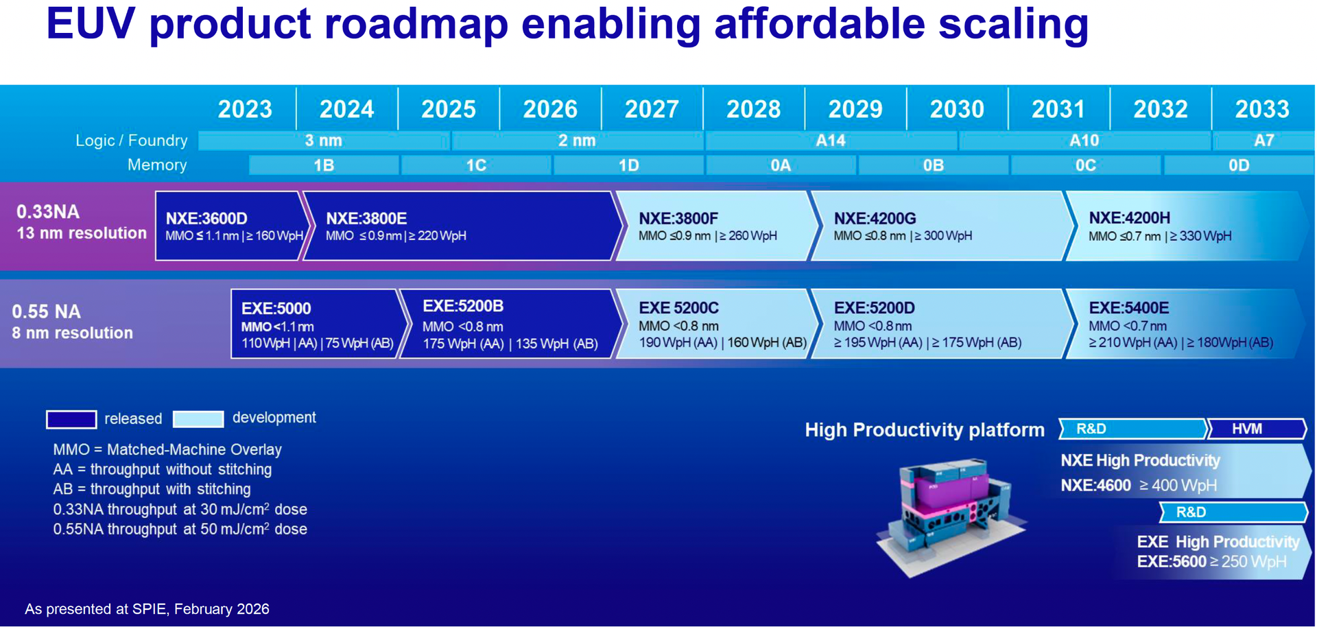
Although Samsung has purchased an ASML Twinscan EXE:5000 EUV lithography scanner with 0.55 numerical aperture projection optics and has been using it for research purposes for well over a year, the company is not in any rush to adopt High-NA EUV lithography for its 2nm-class and 1.4nm-class fabrication technologies. Samsung only plans to insert such a tool for its 1nm-class process sometime in 2030.
"We wanted to apply High-NA EUV to mass production at nodes such as 2nm and 1.4nm, but the technology still requires further improvements," said Chang Min Park, Master VP of Technology at Samsung Electronics, at the conference. "We believe High-NA EUV will become necessary from A10 and below, and we are conducting joint development with various partners."
For chipmakers, the main challenge with ASML's High-NA EUV tools are substantially higher costs compared to Low-NA EUV systems used today, which greatly increases costs of fabs and can affect costs of chips. Meanwhile, High-NA EUV scanners introduce a smaller exposure field, which can require die stitching for large chips and complicate designs, which largely diminish their performance advantage over regular Low-NA EUV systems that stems on reducing the need for using multipatterning.
In addition, High-NA EUV needs improved photoresists, different masks, pellicles, metrology, inspection, and computational lithography, just to name some of the requirements. As a result, chipmakers must determine when it makes sense for them to use expensive single-patterning on High-NA EUV tools and when they can live with increasingly mature 0.33-NA EUV multi-patterning. For example, Intel intends use High-NA EUV tools with some of its 14A technologies, whereas TSMC looks at High-NA EUV lithography as on technology for the 2030s.
Intel CEO Lip-Bu Tan has revealed that new memory architectures — once thought a commodity business — are now strategically interesting and one of his pet projects, while speaking about the comeback of the American chip industry. He further noted that the memory industry is ripe for innovation, and also hinted at exploring ways to stack memory on top of a CPU.
After years of being a commodity, memory became a strategic asset in recent quarters and will likely remain one for a while, so suddenly, leading makers of 3D NAND and DRAM became highly profitable companies, something the Intel CEO is keenly aware of: "I used to be, 'do not invest in memory because it is a kind of commodity business,' but now it has become different," Tan said. […] "There is a lot of new technology coming out. So, we are kind of looking at one of my pet projects, some of the new memory architecture. I think you just saw the news: I hired my good friend, Seok-Hee Lee, who used to run SK Hynix. So, you kind of know something that I am thinking about. We are not ready to unfold it."
Tan did not reveal anything about the pet project and did not even specify whether the project is one of his personally favored strategic initiatives at Intel, or an initiative in one of the companies that he has invested in. He did mention that stacking memory on top of a CPU could make a lot of sense, though did not elaborate. Tan's remarks also follow the revelation of an Intel XBM patent that does away with the silicon interposer of HBM.
" I think CPU and memory, I think there are a lot of ways we can really do stacking together," Tan said. "And also try to find some new architecture for memory. I think in some way the memory, a lot of innovation are not there. So, there is some really good area."
Not everyone in the industry remembers, but Intel started as a memory company in 1968 and was quite a successful memory maker until the eighties, when Japanese companies took the lead, and Intel had to exit the market completely after suffering severe losses. Since then, the company has attempted either to return to the memory market with NAND and Optane, or at least to capitalize on a new type of memory with RDRAM. In all three cases, the company abandoned its memory initiatives without incurring significant losses.
Given the current profitability of 3D NAND and DRAM makers, producing memory is certainly a good business again and will remain profitable for some time. However, to re-enter it, companies like Intel would need capital to build at least one fab, R&D to develop competitive process technologies, and time. While licensing a technology — assuming that a company has capital — is an option, we strongly doubt that at this point Intel may be inclined to invest capital in memory and not in its core products and foundry businesses. Furthermore, it is unclear how investors react to such investments given the fact that the company struggles to become a strong competitor in the foundry market and has exited 3D NAND and 3DXPoint/Optane businesses after failing to achieve strategic targets.
SK hynix has resumed investments in its fab in Dalian, China, which is operated by its Solidigm subsidiary, and plans to boost its output by 50% already in 2027, reports Sedaily. Coincidentally, the company is mulling listing some of Solidigm's shares on NASDAQ to raise capital, but to retain control over its North America-based subsidiary, according to The Korea Herald.
After SK hynix acquired Intel's 3D NAND and SSD business in 2021 and formed its Solidigm subsidiary shortly after, it suspended any expansions of Solidigm's capacity in China partly due to the memory market downturn in 2022 – 2023 and partly due to U.S. export controls that curb exports of advanced fab tools to China. However, as demand for solid-state storage is setting records in general and demand for Solidigm's high-capacity SSDs is exceptionally strong, SK hynix is reconsidering its capacity plans for the Dalian fab just in time for Solidigm's initial public offering.
Following a four-year pause, Solidigm has reportedly resumed investment in its Dalian facility in China this year. The company has completed construction of the second phase of the fab and is preparing to start installing production equipment as early as November, the report claims. The facility is expected to begin mass production of floating gate 3D NAND flash in the first half of 2027, if the report is accurate.
The second phase of Solidigm's fab in Dalian is reportedly designed for a wafer output capacity of around 50,000 wafer starts per month (WSPM). Combined with approximately 100,000 WSPM at the existing first phase of the facility, the new phase would boost Solidigm's NAND production capacity in Dalian by roughly 50%, to around 150,000 WSPM.
Late last year, the U.S. government granted SK hynix and Samsung annual licenses to ship semiconductor production equipment that contains technologies developed in America to their Chinese fabs through 2026, which replaced their previous open-ended Validated End User (VEU) exemptions. As a result, both companies can now upgrade their fabs in the People's Republic and even use new process technologies there.
Solidigm, for example, intends to start making floating gate 3D QLC NAND memory with over 200 active layers at its Dalian facility in the second half of 2026, which was made possible by the timely tool upgrades. The additional capacity will further increase bit output of the Dalian campus, which in turn will enable Solidigm to produce its 245TB-class SSDs due to be introduced in the coming months in decent quantities, sometimes in 2027.
Solidigm, which controls roughly a quarter of the data center-grade SSD market, is a crown jewel in SK hynix's portfolio as it makes unique products that are sold at a premium and are in high demand. Listing Solidigm on NASDAQ would enable SK hynix to gain capital (up to $7 billion, if unofficial reports are correct), but retain control over the precious asset. The money that SK hynix will raise should be roughly enough to expand Solidigm's capacity and increase output of premium data center-grade solid-state drives.
It should be noted that SK hynix did not officially confirm the Solidigm IPO plan last week, as its regulatory filing on August 5 said that Solidigm was considering various ways to improve its competitiveness, but the final decision is yet to be made.
Intel is set to raise $19.7 billion by selling new common stock in a bid to finance the building out of new production capacity, the development of next-generation leading-edge process technologies like 14A and others, and day-to-day operations. While the company does not assign money to a particular project, Intel needs to build capacity to land orders from large external clients, so capacity expansion will likely be a priority. According to Bloomberg, the share sale attracted $100 billion in demand.
Intel will sell 210,526,315 shares for $95 apiece through an underwritten public offering. In addition, participating banks have 30 days to acquire as many as 31,578,947 more shares at the same $95 price, minus applicable underwriting discounts. Should they exercise all their options, Intel could sell approximately 242.1 million shares altogether and increase the proceeds to roughly $23 billion. Without the additional shares, Intel expects net proceeds of approximately $19.7 billion after underwriting discounts, commissions, and estimated expenses. The transaction is scheduled to close on August 12, 2026.
Intel's market capitalization increased from roughly $90 billion last August to $491 billion at press time, so the time is right to sell some shares and raise some much-needed cash, as the company must compete against giants like TSMC and Samsung, which spend tens of billions of dollars every year on new fabs and advanced process technologies. Meanwhile, Intel's capitalization reached its all-time high of $673 billion on June 20, 2026.
Intel has not assigned the money it is going to raise to particular projects and says the capital can be used across the business, including for capital expenditures and working capital. The company is currently ramping up its Fab 52 in Arizona and is on track to start using adjacent Fab 62 when it needs to. In addition, the company still has to build its fab complex in Ohio, which is expected to cost over $100 billion when fully built, so it badly needs money.
In its risk disclosures, the company specifically mentioned Intel 14A — which is due to enter mass production in 2028 — and other advanced process technologies, manufacturing expansion required to support them, and the need to secure design wins and volume commitments from major external foundry customers. While Intel does caution that these long-term investments amounting to tens of billions may not generate adequate returns, it is impossible to land sizeable contracts from external customers without having production capacity readily available.
Interestingly, Intel also mentioned alternative financing arrangements, government grants, and the U.S. government's significant equity position in the company among relevant factors.
House Select Committee on China Chairman John Moolenaar has written a letter that demands the U.S. government enforce an existing export control measure designed to prevent Chinese companies from getting advanced chips produced by contract chipmakers like TSMC or Samsung Foundry.
When Joe Biden was about to leave the office in early 2025, he signed a law that required chipmakers to determine their end customers in a bid to prevent contract manufacturers from unknowingly fabricating chips using American technologies for companies that served as intermediaries for restricted organizations tied to the Communist Party or the People Liberation Army. The regulation was introduced after it was discovered that chips made by TSMC for China-based Sophgo were actually Huawei's Ascend 910B AI accelerators. However, the Trump administration announced in May 2025 that it would not enforce this semiconductor regulation known as the 'Foundry Due Diligence Rule,' which naturally created uncertainty about whether the foundry-focused requirements would be actively implemented at all.
"The announcement created ambiguity as to whether front-end fabricators like TSMC can export unpackaged advanced dies to non-approved designers located outside of China, without performing the due diligence specified in the Foundry Due Diligence Interim Final Rule (IFR)," the letter reads. "These exports enabled Huawei to obtain millions of controlled Ascend logic dies from TSMC, using its front company, Sophgo in 2023 and 2024."
Before the adoption of the 'Foundry Due Diligence Rule,' Chinese companies and/or their intermediaries could misrepresent chip specifications and end users when placing orders with TSMC or other foundries, which allowed restricted devices to be made despite U.S. export controls. Under the rule, foundries and OSAT providers exporting chips produced on 14/16nm-class process technologies or more advanced nodes must presume those devices qualify as controlled AI processors subject to a global licensing requirement, unless they meet an exemption. According to the letter, foundries have generally complied with these requirements since the rule took effect. As a result, Moolenaar essentially asks the government to enforce the existing controls rather than introduce stricter export controls.
Moolenaar believes that the Commerce Department's Bureau of Industry and Security could clarify its current stance on the Foundry Due Diligence Rule in two ways:
By issuing guidance, which confirms that the worldwide Regional Stability (RS) licensing requirement still applies to exports from front-end foundries;
By formally annulling the AI Diffusion IFR and amending §744.23 to explicitly restore that requirement for both foundries and OSAT providers.
Either approach would eliminate conflicting interpretations and reinforce enforcement of existing export controls, Moolenaar believes.
Nvidia late on Monday announced that it had signed memorandums of understanding with Apollo, BlackRock, Blackstone, Brookfield, Goldman Sachs, and KKR to establish independent financing platforms that could mobilize more than $500 billion in third-party capital to invest in AI infrastructure. Nvidia's goal is to ensure that its clients building AI data centers (which Nvidia calls AI factories) can get enough money from powerful financial companies. As a result, Nvidia will reinforce its position on the AI hardware market as the funds will exclusively finance Nvidia-based AI data centers.
The proposed funds (or platforms, as Nvidia calls them) are intended to provide dedicated pools of capital for customers — such as AI labs, cloud service providers, or enterprises — that deploy Nvidia-based infrastructure. Rather than financing projects itself, Nvidia intends to work with six investment firms to enable access to long-term funding at attractive rates. The company believes that AI infrastructure should not be viewed as conventional IT equipment, but as tools that make sustained economic returns, which is why it must be financed appropriately.
"We are in a pivotal moment of a historic AI investment cycle," said David Solomon, Chairman and CEO of Goldman Sachs. "Nvidia's full-stack platform is in high demand and uniquely positioned at the center of that global buildout. Our investment and distribution roles reflect our confidence in Nvidia's leadership, and we are excited for the new opportunity to create a market for credit backed by NVIDIA compute."
The financial companies believe that AI data centers can be treated as long-duration infrastructure assets rather than conventional IT equipment, in part because Nvidia compute can generate revenue over an extended period and retain value across different workloads and operators. As a result, they appear to believe that AI infrastructure can support long-term financing at attractive rates, although the companies do not explicitly claim that financing AI data centers carries lower credit risk than financing conventional IT deployments. Furthermore, it should be noted that Nvidia and financial companies will inevitably finance companies that would otherwise struggle to obtain capital to finance their AI data centers. This will ultimately help Nvidia sell more hardware and software while allowing its financial partners to capitalize on the rapid expansion of Nvidia's AI ecosystem.
Without any doubt, the arrangement will help to rapidly build AI infrastructure, which will increase adoption of AI technologies. However, this arrangement increases the risk of an AI infrastructure bubble as it potentially weakens one of the natural brakes on overbuilding: the availability and price of capital. Furthermore, Nvidia's help with arranging financing for its own customers introduces an element of circular financing into the AI boom, something that the industry faced during the dot-com bubble era in the late 1990s – early 2000s. However, this does not necessarily prove there is a bubble, as there is genuine, enormous demand for AI hardware and Nvidia sells plenty of such hardware.
Perhaps the biggest concern about the arrangement is that while Nvidia and its partners state that AI infrastructure can provide long-term value, AI accelerators, such as Nvidia's GPUs, have short and uncertain economic lives as the company and its industry peers introduce new and better-performing AI hardware every year, which devalues the previous generation.
"Nvidia has reached an important milestone: we began by building chips; today, we are helping create a new class of productive, investable infrastructure: AI factories," said Jensen Huang, founder and CEO of Nvidia. "In AI, compute is revenue. Nvidia compute is uniquely suited for this role. It is broadly adopted, flexible across models and workloads, fungible and transferable across customers and operators, and continuously improved through CUDA software — extending its useful life and improving its economics over time. It is supported by a deep global ecosystem of developers, customers, and offtakers. That is why we are bringing the world's leading long-term capital providers together to independently underwrite AI infrastructure. These financing platforms will help customers access scarce compute at scale and build the DSX AI factories that will power every industry and country in the age of AI."
Apple used to be among a few companies willing to buy memory and other components worth billions of dollars under long-term supply contracts at fixed prices. But the artificial intelligence era represents a new reality with new purchasing champions, marking a tectonic shift in the high-tech world. Alphabet, Microsoft, Meta, and Amazon have purchase commitments totaling about $2 trillion, and a significant portion of these commitments are for memory, according to estimates by analyst Claus Aasholm. While the commitments are approximate, span many years, and should be generally taken with a grain of salt, they still reflect the direction the industry is moving.
Combined purchasing commitments from the four major hyperscalers shown in the chart —Amazon, Alphabet, Meta, and Microsoft — reached nearly $2 trillion by Q2 2026, with Alphabet and Microsoft accounting for the overwhelming majority of the total.
The rapid expansion suggests several major findings. Firstly, the AI infrastructure race is accelerating, not stabilizing. Secondly, AI infrastructure investments are driven by a handful of hyperscale cloud service providers (CSPs) whose long-term procurement commitments now vastly exceed those of traditional consumer electronics companies such as Apple.
Thirdly, memory has become a strategic asset — perhaps a competition weapon — rather than a commodity. Fourthly, suppliers of memory — both 3D NAND and DRAM — are gaining pricing power. Finally, demand for memory will likely drive major capacity expansion at Micron, Samsung, and SK hynix, even though so far these companies have been exceptionally disciplined about their capacity investments.
Almost $2 trillion commitments
Google shows by far the most aggressive increase in purchasing commitments, rising from roughly $140 – $150 billion in Q3 2025 to around $811 billion by Q2 2026 (though these are total purchase commitments by Alphabet, not specifically memory purchase commitments), while Microsoft follows a similar trajectory and reaches approximately $678 billion in total obligations, which includes, but is not limited to memory.
Meta is also ramping commitments substantially to around $349.3 billion (again, these are total commitments), whereas Amazon increased its commitments more gradually to roughly $130 billion. By contrast, Apple — which makes the world's most popular smartphone, and which was the largest consumer of memory just a couple of years ago — remains almost flat throughout the period at approximately $57 billion (of which $56.2 billion is payable within 12 months). Apple's commitments fall well short of Nvidia's commitments of $119 billion.
Memory suppliers used to buzz around Apple like fruit flies, but now they have discovered larger commitments.Apple's purchasing commitments have not changed, suggesting a reluctance to follow the new market rules.https://t.co/0pRbk8aYVJ pic.twitter.com/t2VNm7uw1dAugust 6, 2026
Again, we are talking about total purchase commitments, which include foundry capacity, 3D NAND, and DRAM memory, but are not limited to them. Alphabet, Amazon, Meta, and Microsoft all build custom silicon and custom servers, so a significant portion of these commitments is to various EMS providers.
While $1.968 trillion of purchase commitments for memory and storage alone would be an absurdly large amount of money, a huge portion of these commitments consists of contract manufacturing obligations as well as memory chips. This suggests that the foundry, 3D NAND, and DRAM markets are entering a new phase in which hyperscalers are willing to make vastly larger forward purchasing commitments than traditional consumer-electronics companies, giving suppliers a strong incentive to prioritize customers prepared to secure future capacity on that scale.
Strategic assets
While Claus Aasholm's chart is explicitly dedicated to memory, it does describe total purchase commitments of tech giants, so the chart can reasonably be read as evidence that memory and capacity at TSMC, Samsung Foundry, and GlobalFoundries are becoming a strategic asset rather than merely another component to procure at the best available price.
AI infrastructure requires enormous quantities of AI accelerators, DRAM (including HBM), and 3D NAND. Meanwhile, the supply of high-end memory (HBM) is constrained by fab capacity at major DRAM makers, whereas the supply of AI accelerators is constrained by both wafer capacity and foundries and packaging capacity at foundries and their OSAT partners. As a result, hyperscaler CSPs have an incentive to lock in supply years ahead, even if doing so requires exceptionally large purchasing commitments.
That also changes the relationship between semiconductor suppliers and their customers. In theory, a company willing to guarantee hundreds of billions of dollars of future purchases can effectively help underwrite expansions of foundry, memory, and advanced packaging capacity and, in return, secure priority access to scarce products and future process technologies. In reality, TSMC can well afford capacity expansion using the money it gets from hyperscalers and give priority to its largest customers. In this environment, access to DDR5, HBM, and 3D NAND memory becomes part of the competitive advantage rather than merely a procurement exercise.
This is also what makes Apple's position in the graph interesting: its purchasing commitments barely move while those of Alphabet, Amazon, Meta, and Microsoft surge. If the trend continues, Apple may remain one of the world's largest semiconductor buyers in absolute terms, but the question is whether it will be among the key customers that foundries, memory makers, and OSATs plan their future capacity expansions.
An inflection point
Perhaps the most interesting takeaway of the findings revealed by long-term purchase commitments is that the industry's center of gravity appears to have shifted.
During the smartphone era, foundries (well, TSMC has won) and memory suppliers often competed aggressively for Apple's business because of its enormous purchasing power. Today, hyperscalers building AI infrastructure are making purchasing commitments that dwarf those of traditional CE companies like Apple, which may well represent a strategic inflection point akin to the one Andy Grove described in his 'Only the Paranoid Survive' book.
Will this tectonic shift result in prioritization of customers capable of enabling future capacity expansions through massive long-term purchase agreements, or will foundries and memory makers remain more or less disciplined with their capacity expansions so as not to lose a lot when demand declines? This is a question that has yet to be asked.
In any case, the AI megatrend has transformed semiconductors — from foundries to advanced packaging and from DDR5 to HBM4 — into strategic assets that can no longer be treated as ordinary components procured on demand. And this is something that will continue in the long run.
SpaceX and Tesla on Thursday formally unveiled plans for the initial phase of their Terafab project. The first stage of the plan — which is expected to use Intel's 14A process technology — is expected to require $16.8 billion in investment, while the completed campus is planned to encompass more than 100 million square feet of manufacturing space. The massive semiconductor manufacturing complex will be built in Grimes County, Texas, at a location that belongs to SpaceX.
According to SpaceX and Tesla, their combined demand for semiconductors is projected to exceed 1 terawatt (TW) of compute per year, which significantly exceeds today's global supply. In fact, SpaceX, Tesla, and xAI already consume a significant portion of contract chipmaking services available today, and can potentially justify building a dedicated fab that will exclusively serve Elon Musk's companies. In particular, Terafab is envisioned to exclusively produce AI inference processors for Tesla Optimus humanoid robots and Cybercab autonomous vehicles, as well as 'high-power' processors intended for SpaceX's space-based data centers. Meanwhile, SpaceX and Tesla have not disclosed when their combined demand for compute per year will hit the 1 TW benchmark.
Unlike a conventional semiconductor fab, Terafab is envisioned as a vertically integrated manufacturing campus where advanced logic devices, memory chips, packaging, and testing operations are housed together. Normally, logic and memory are produced at different fabs using different process technologies, whereas packaging and testing services are performed at different facilities. However, the companies believe that consolidating logic, memory, packaging, and testing in one location will not only shorten the production cycle but will also shorten time-to-yield by enabling faster iterative improvements.
Given the description and the goal of the project, this will be a massive facility. Yet, SpaceX and Tesla have said little about its capabilities; The only thing they have disclosed is that the current facility in Grimes County will feature '100 million square feet of manufacturing space.' The 100 million square feet (9.3 million square meters) figure immediately stands out because it is far beyond anything ever announced for a semiconductor manufacturing facility. For example, the total area of Samsung's Pyeongtaek campus is approximately 2.89 million square meters, or 31.1 million square feet. A single Samsung fab occupies about 120,000 square meters, or 1.29 million square feet. However, the key wording is important: '100 million square feet of manufacturing space' does not mean 100 million square feet of cleanroom space.
Based on an image published by SpaceX, the Terafab facility will occupy four massive buildings. It is unclear whether these buildings will be four phases of the project (i.e., logic, memory, and packaging will be made under one roof) or will serve different purposes (i.e., one building makes logic, another produces memory, yet another does testing and packaging). In any case, when fully built, Terafab will be a massive semiconductor production campus that will require significantly more than $16.8 billion.
The announcement claims that the Terafab facility will employ at least 3,000 people, and that between 60% and 80% of them will be Grimes and nearby Brazos County residents.
Terafab is expected to use water from Gibbons Creek Reservoir instead of local groundwater and feature on-site wastewater treatment as well as water recycling and conservation measures.
The announcement follows Tesla's groundbreaking earlier this year on a research semiconductor facility at the North Campus of Tesla's Giga Texas campus, which the companies describe as a precursor to Terafab.
This week, Samsung presented its vision for next-generation memory and storage solutions both for AI and general-purpose applications at the Future of Memory and Storage (FMS) 2026 conference. The company introduced zHBM, zNAND-O, and BV-NAND technologies at the event, and while they are aimed at very different applications, they share one common ingredient: they all rely on wafer bonding.
Here's a breakdown of each type of technology that the company announced.
zHBM: Samsung’s vision for custom HBM ultra-high-performance memory that will sit on top of logic dies.
zNAND-O: NAND memory that can be bonded atop a logic device to maximize bandwidth, reduce latency, and minimize power consumption.
BV-NAND (aka Samsung’s 10th Generation V-NAND): Samsung’s take on bonding NAND arrays atop all the circuitry needed to operate them. This is essentially next-generation 3D NAND technology that is used today by almost everyone, including Kioxia/Sandisk, SK Hynix, and YMTC (which was the first company to adopt such a method).
This article is a preview of the type of content that readers can expect from our subscription service, Tom's Hardware Premium. If you're interested in more technical content that spans across the hardware industry, subscribe for as little as $29 per year, or $7 per month.
Don’t miss out on this Tom’s Hardware Premium. Get a full year of access for just $29, or from $7 per month. Get daily news analysis, deep dives into specialist topics in the semiconductor industry, as well as access to Bench, the largest benchmarking database around.View Deal
zHBM: Placing HBM stack on top of logic
Around the time we first heard about HBM4's 2,048-bit interface, we read a 'semi-official' report that SK hynix and its partners were considering vertical integration of HBM4 stacks on top of logic chips. To a large degree, companies were considering installing these memory stacks on top of their processors as they doubted that it would be possible and feasible to use interposers to connect HBM4 stacks to AI accelerators. Over time, it turned out that integration of memory on top of logic is complicated when it comes to cooling, power delivery, and developing interposers that can handle a 2,048-bit memory interface. Samsung's zHBM appears to be a continuation of that effort.
(Image credit: Samsung)
Samsung's zHBM concept places HBM directly on top of an AI accelerator instead of on its perimeter, which greatly reduces the distance data must travel between compute and memory. The company says this architecture can increase bandwidth and power efficiency and projects that it can provide 8x the 'performance of HBM5', while its advanced wafer bonding is expected to enable over 10x higher memory density, 3x better energy efficiency, and more than 50% lower thermal resistance than HBM5.
While Samsung's claims about the zHBM look incredibly impressive, they are vague. For example, when the company claims that a 'next-generation interface system incorporating zHBM' will deliver 'approximately eight times the performance of HBM5,' it never explicitly states whether this refers to memory bandwidth, actual application performance due to a combination of improvements over standard HBM, or something else. Had Samsung intended to compare raw bandwidth, it would likely have used more precise wording, such as '8x higher bandwidth.'
Instead, the general term 'performance' may have many meanings. The same applies to references of improved power efficiency, higher memory density, and lower thermal resistance compared to HBM5, a standard that has not been fully defined or ratified. To make matters even more imprecise, Samsung mentions thermal resistance, which depends on implementation rather than the standard. Finally, Samsung didn't reveal which die stacking/bonding technology it will use for zHBM.
In any case, Samsung says that zHBM will also support customer-specific designs and will enable custom IP to be integrated into the interconnect layer (which plays a role similar to the base die, though it is definitely not a base die per se) between the HBM stack and the AI processor, which essentially means that zHBM is not necessarily an industry-standard solution, so it might be implemented with additional perks.
For now, Samsung hasn't disclosed any timeframes for when it plans to offer its zHBM solutions. The only clue is that it compares it to HBM5, which is likely to see the light of day sometime in the late 2020s or early 2030s.
zNAND-O(on-device): Put storage close to compute
Samsung also unveiled zNAND-O, a high-performance NAND memory currently in development that will enable putting four or eight stacks of NAND devices on top of logic dies. zNAND-O(n) device is based on the company's V-NAND platform (or rather, BV-NAND) and is meant to combine high storage density with improved I/O performance and low latency.
(Image credit: Samsung)
Samsung claims that the tech is suitable for edge AI systems running real-time, data-intensive inference workloads, though, of course, there are many other applications that can benefit from high-performance on-package storage.
(Image credit: Samsung)
Since the technology is in development, Samsung hasn't shared much information about it, even keeping the schematics of how it plans to put zNAND-O layers on top of a logic under wraps. We can speculate that since Samsung mentions 'improved I/O performance and low-latency,' it may be planning to exploit both the inherently parallel architecture of NAND memory with a high-performance interface, though we will not try to dive into details for the sake of not making the discussion too speculative.
BV-NAND: Good old V-NAND gets a new treatment
With BV-NAND, Samsung is essentially introducing a new brand name for its next-generation 3D NAND that bonds the NAND array on top of the I/O and logic wafer. This, in turn, produces the layer itself using high-performance logic process technologies and enables higher I/O speeds.
(Image credit: Samsung)
Samsung formally announced its 400-layer-class V-NAND (aka 10th Generation V-NAND) some time ago, and even disclosed that its areal density would be 28 Gb/mm2 with a maximum I/O speed reaching 5600 MT/s. This likely stipulates the usage of a pinout that is different from the 3D NAND packages used today. While the areal density of Samsung's 10th Gen TLC V-NAND is slightly lower when compared to that of Kioxia/Sandisk's BiCS10 TLC NAND, its maximum I/O speed is significantly higher, which perhaps justifies the new branding.
NAND Layer Counts
Samsung
Samsung
Sandisk/Kioxia
Sandisk/Kioxia
Kioxia/Sandisk
Micron
SK hynix
YMTC
YMTC
Generation
V10
V9
BiCS10
BiCS10
BiCS 8
Gen 9 (G9)
Gen 9
?
Xtacking 3.0/Gen 4
Layers
4xx-Layer
290-Layer (?)
332-Layer
332-Layer
218-Layer
276-Layer
321-Layer
232-Layer
232-Layer
Density
28 Gb mm^2
17 Gb mm^2
>37 Gb/mm^2
>29 Gb/mm^2
22.9 Gb mm^2 (?)
21.0 Gb mm^2
20 mm^2
>20 Gb mm^2
19.8 Gb mm^2
Architecture
TLC
TLC
QLC
TLC
QLC
TLC
TLC
TLC
QLC
Die Capacity
1 Tb
1 Tb
?
1 Tb
2 Tb
1 Tb
1 Tb
1 Tb
1 Tb
I/O Speed
Up to 5600 MT/s
Up to 3200 MT/s
Up to 4800 MT/s
Up to 4800 MT/s
Up to 3600 MT/s
Up to 3600 MT/s
?
?
?
Considering the fact that Samsung rarely sells its memory to third parties and prefers to market client SSDs itself, a new brand for memory can be a sales driver, even if actual high-end drive performance is limited by a PCIe 5.0 x4 interface rather than by 3D NAND memory I/O. Then again, the performance of mid-range PCIe Gen5 SSDs that rely on a quad-channel NAND controller depends on 3D NAND I/O today, so marketing them under a new flash memory brand is a certain way to attract attention and then sell decent performance.
Samsung's new brand strategy
As the new name of the FMS tradeshow implies, the announcements touch upon very distinct industry needs. In the case of Samsung, we are talking about high-performance data center-grade AI accelerators; applications that need storage with latency that is lower than ~50 – 60 µs of modern high-end PCIe SSDs, though we will see how it compares to Z-NAND, and essentially a new generation of conventional 3D NAND with a new brand.
Except for the 400-layer-class Samsung BV-NAND that is set to hit the market in the foreseeable future, the company's new tech, like zHBM and zNAND-O, is years away.
Following its massive $8.6 billion initial public offering (IPO) in July, ChangXin Memory Technologies (CXMT) began considering building its sixth DRAM fab in China to boost memory output in the coming years, Reuters reports. If all announced projects proceed as planned, the company's production capacity could more than double in the mid-term future, the report claims. Meanwhile, investment banker Dan Niles believes China could capture 30% of the DRAM market by 2030, according toP Equity Research.
Growing at a rapid pace
CXMT currently operates three 300-mm DRAM fabs: two near Hefei and one in Beijing's Yizhuang district. Unofficial reports claim that each fab is capable of processing around 100,000 wafers per month, so the company's output may be around 300,000 wafer starts per month (WSPM).
(Image credit: CXMT)
The company is pursuing an aggressive expansion strategy and is currently building additional fabs near Shanghai and Hefei, according to Reuters. The company's sixth fab will reportedly be located in Beijing's Yizhuang area, adjacent to its existing facility. Once these projects are fully operational, the company’s total manufacturing capacity could exceed 600,000 WSPM, which will double its current output, according to Reuters. Meanwhile, researchers from Citrini believe that CXMT could exit 2026 with a capacity of 350,000 WSPM, which is just 25,000 WSPM shy of what Micron targets by the end of the year. Citrini Research models that by 2030, CXMT will have production capacity of around 950,000 WSPM.
Building three big DRAM fabs is a big deal, from both financial and execution points of view. However, it is not a secret that virtually all fabs owned by Chinese companies are built using money from local and federal governments under the 'Hefei model,' which aims to transform cities into economic juggernauts by leveraging high-risk projects. So it is not surprising that both Shanghai and Beijing have provided financial assistance and other forms of support to attract CXMT to their regions, according to Reuters.
CXMT's existing Beijing fab, operated by Changxin Jidian, received backing from E-Town Capital and Beijing E-Town Technology, both affiliated with the Yizhuang development zone, according to a person familiar with the matter cited by Reuters. In fact, the district has evolved into a relatively major semiconductor manufacturing hub that already hosts CXMT, SMIC, Naura Technology, and Xiaomi, the report claims.
The right timing
The proposed fab would be located in Beijing's Yizhuang district, roughly 20 kilometers southeast of the city center, where CXMT already operates a 300-mm DRAM manufacturing facility. The planned production capacity and total capital investment for the project have not yet been disclosed, although Reuters points out that a leading-edge DRAM fab typically costs well over $10 billion.
(Image credit: CXMT)
Sources cited within the report said the company is seeking at least 60 million yuan ($8.9 million) in financial support from the Beijing Economic-Technological Development Area, and additional state-owned technology companies have also expressed interest in participating. Discussions remain preliminary, and neither the overall size nor the structure of the financing package has been finalized.
From CXMT's point of view, this is the right time for financial influxes as the company can sell all of its DRAM output at good prices to a variety of customers. Those being domestic PC and server makers (including Lenovo), and global brands such as Micron, Samsung, and SK hynix, which prioritize shipments of their DRAM output to the AI sector.
Apple, Dell, and HP have all reportedly qualified CXMT's memory and are ready to deploy it in their devices sold in China, while Acer and Asus have already begun to use DRAM from the Chinese maker. If CXMT signs long-term supply contracts with the world's leading PC makers, it is nearly guaranteed to sell out its output to these vendors in the coming years, which justifies investments in its expansion.
30% of DRAM market by 2030?
Dan Niles, founder of Niles Investment Management, believes that many investors underestimate how much share CXMT could capture over the coming years and how much share China may seize in the coming years.
(Image credit: Samsung)
His argument stems from historical DRAM market leadership shifts. In 1975, U.S. companies controlled 95% of the DRAM market, with Intel alone holding 75%. Japan then turned DRAM into a commodity business, increased its share to 80% by 1985, while the U.S. fell to 10% and then just 2% by 1990. Then South Korea repeated that playbook in the mid-1980s and eventually displaced Japanese suppliers, and today it accounts for roughly 62% of the global DRAM production.
With Micron's investments of hundreds of billions of dollars in U.S. DRAM capacity, the country is set to regain its massive presence on the global DRAM scene; China could capture 30% of the market by 2030, according to Niles.
China already consumes around 30% of global memory output, as it produces hundreds of millions of PCs and smartphones both for domestic and global consumption; it is reasonable to expect the country to produce as much commodity memory locally as possible. Keeping in mind China's push for semiconductor self-sufficiency and willingness to invest huge amounts of money in domestic fabs, it is possible to expect the country to rapidly gain DRAM output and share. China is already pushing its chipmakers hard to start DRAM production, and the government reportedly asked CXMT to share its process technologies with others.
Not that easy
There are multiple factors — both technological and political — that may, if not stop, but greatly slow down CXMT's and China's DRAM expansions in the coming years.
(Image credit: Micron)
First up, there are export controls in place that prevent Chinese entities from getting sophisticated wafer fab equipment required to make DRAM using 18nm-class process technology or more advanced. If the proposed MATCH Act passes, then limitations on Chinese companies will get more severe, which will reduce their expansion ability.
Secondly, even if CXMT (or another Chinese DRAM maker) finds a way to produce more advanced DRAM using relatively outdated tools (i.e., use old tools for sub-16nm nodes), they will need to acquire those tools in quantity to increase their output. Meanwhile, companies like ASML have relatively limited production capacities, and CXMT is certainly not the only memory maker seeking to expand its production capacity in the coming years. While SMEE and SiCarrier are developing lithography tools in China, they will be unlikely to ramp up production of immersion DUV scanners to higher levels any time soon.
Thirdly, building fabs is one thing; operating leading-edge DRAM production at high yields is another. China has recruited engineers from Micron, Samsung, SK hynix, and TSMC for years, but scaling from three to six or more fabs requires thousands of experienced process, yield, device, lithography, and integration engineers. Building fabs adjacent to existing sites enables CXMT and other chipmakers to share experience and knowledge internally, which helps to develop experienced talent. But will it be enough for the long term?
Next, expanding wafer capacity alone is insufficient. DRAM producers must continuously migrate to finer process technologies (e.g., 16nm-class, 14nm-class, 12nm-class) to remain cost-competitive. If export controls delay access to equipment or materials needed for these nodes, Chinese fabs could end up producing more wafers at a higher cost per bit than competitors.
Finally, some American lawmakers want to prohibit U.S.-based companies from acquiring memory from CXMT and other Chinese vendors. They have every reason to believe that China wants to take control of a sizeable DRAM market share in a bid to use it in its strategic interest and have leverage over the market, something the country already has with rare earth metals. If the lawmakers manage to turn the proposal into law, demand for CXMT's and other China-made DRAM will drop. It will probably be sufficient inside China, but whether it will be enough to justify 10 or more big DRAM fabs is a different question.
Elon Musk on Tuesday said in an X post that SpaceX and xAI will exclusively use Nvidia GPUs because 'they are the best.' He later clarified during SpaceX's earnings call that Nvidia's Vera Rubin NVL72 rack-scale system's design is above everything else that is available today, which is certainly praise for Nvidia, but not such a good sign for other developers of merchant AI accelerators.
SpaceX has committed to using Nvidia GPUs exclusively because they are the bestAugust 4, 2026
"Going forward, we have decided to build exclusively on Nvidia, because we think the Vera Rubin architecture is the best architecture," Elon Musk said during SpaceX's earnings call. "We think it is the best AI computer, and we greatly value our close cooperation and partnership on many levels with Nvidia. We are exclusive to Nvidia. […] We think the design of the NVL72 VR[200] computer is a much better design than, say, having a standard rack style design."
Historically, xAI has exclusively used Nvidia's Hopper and, more recently, Blackwell hardware to train multiple generations of Grok. Although AMD has used Grok-1 on its Instinct MI300X accelerators, there has never been a public announcement or credible evidence that xAI has evaluated or used AMD Instinct, or other non-Nvidia accelerators in production. xAI's Colossus supercomputers have been using Nvidia's accelerators for years, so the official exclusivity looks more like a formality that gives a strong testament for Nvidia rather than a decision that was hard to make.
When it comes to the praise of the cable-less design of compute trays in Nvidia's Vera Rubin NVL72 VR200 rack system, then Musk's admiration of this architecture is understandable, as while expensive, such trays greatly improve serviceability, assembly speed, and reliability by eliminating a large number of manual cable and hose connections that are common sources of installation errors and failures.
Interestingly, but Musk's SpaceX plans to deploy Vera Rubin not only in its own and xAI's data centers, but also in space.
"With respect to the Starmind AI satellite, which will be essentially an optimized Vera Rubin NVL72 computer, this is not some sort of far future distant thing; we expect to start launching this next year," Musk said. "We think the design of the NVL72 VR[200] computer is a much better design than, say, having a standard rack style design. We expect to actually deploy this on the ground as well as in orbit, because we think it is going to be a radical simplification of the normal NVL72 rack."
Deploying an NVL72-scale machine will be by far a more ambitious project than Nvidia has in mind with its Space-1 Vera Rubin Module that is designed to deploy several, perhaps a dozen, of Rubin AI accelerators in space. 36 Vera CPUs and 72 Rubin AI GPUs offer rather formidable performance, though many questions remain about the cooling and reliability of such racks in space.
It is not a secret that proper cooling ensures longevity and enables hardware to demonstrate its full potential. But when it comes to data center AI hardware, proper cooling also means higher sustained performance, which directly translates into money earned by the owner. Frore Systems, a maker of cooling solutions that are made using semiconductor-grade tools, seems to have a perfect idea of how to reduce the temperature of next-generation AI accelerators and increase their performance by 15%.
Frore Systems last week published a white paper which suggests that improvements to the entire cooling stack — from the GPU packaging and thermal interface materials (TIMs) to coldplates and coolant temperatures — can increase token generation per watt by more than 30%. Meanwhile, one of the company's boldest projections based on an analytical thermal model* is that its LiquidJet coldplate technology alone can lower Nvidia Rubin GPU junction temperatures by up to 12°C, which translates into a 10% to 25% improvement in tokens/Watt, while a 10°C reduction could increase token generation by around 15%.
Indeed, modern AI accelerators, such as the upcoming Nvidia Rubin, can dissipate up to 2,400 W, and their die temperatures can easily hit 95°C or more. But while 95°C is not necessarily a problem for silicon longevity, leakage current certainly is. Leakage current rises exponentially with temperature, approximately doubling for every 10°C increase in maximum junction temperature, which is when transistor switching itself also becomes less efficient. As a consequence, hotter GPUs require higher voltages to sustain clocks, which eventually forces Dynamic Voltage and Frequency Scaling (DVFS) to reduce clocks to remain within thermal limits, which in turn will reduce performance and token generation.
(Image credit: Frore Systems)
This all leads to a simple conclusion: the better the cooling, the higher the performance and token output. Which is generally right. However, cooling is not as simple, as it depends on multiple factors that can be optimized. Furthermore, for AI data centers, cooling itself is no longer a way to preserve CPUs and accelerators from overheating, but really is a way to maximize their performance and token money generation.
Nvidia designs its platforms around Tj(max) temperature; it is one of the fundamental design constraints for the GPU, package, and cooling solution. This works like this:
Nvidia specifies a maximum allowable junction temperature (Tj,max limit). This is the temperature the silicon must not exceed during normal operation. The exact value is not always public, but Frore uses 95°C for Rubin in its analysis.
The GPU continuously monitors its junction temperature using tens or hundreds of on-die thermal sensors, yet power management monitors the hottest region.
DVFS attempts to maximize performance while staying below the thermal and power limits, so if the GPU has thermal headroom, it can sustain higher clocks or lower voltage. If the junction temperature rises, the firmware gradually adjusts voltage and frequency. If necessary, it throttles to prevent exceeding Tj(max).
The problem is that GPUs operate under several simultaneous limits, such as thermal limit (Tj,max), package power limit, current limit, and voltage limit. Usually, power is reached before thermal. Meanwhile, modern cooling systems are designed to prevent silicon from reaching Tj(max). So, even if Nvidia's GPU never reaches Tj(max), lowering the operating junction temperature still improves efficiency because transistor leakage decreases as temperature falls. This is where Frore and its cooling systems come into play.
According to Frore, leakage power approximately doubles for every 10°C increase in junction temperature, while transistor switching power rises by about 2% over the same temperature range, so lowering operating temperatures is beneficial even when the processor is not thermally throttling.
Thermal resistance
According to Frore, the maximum GPU junction temperature used by hardware makers is directed by a deceptively simple equation:
Tj(max) = Tinlet + Q × Rtotal
where coolant inlet temperature, GPU power, and total thermal resistance determine how hot the silicon can be. Meanwhile, total thermal resistance depends on three major elements: the GPU package itself, the thermal interface material between the package, and the coldplate design. As each layer adds thermal resistance, it increases die temperature and reduces overall token money generation. That said, thermal resistance is becoming a major problem, according to the paper.
Frore claims that delidding the Rubin package dramatically lowers thermal resistance (while this is obvious, I must add again that the paper is based on an analytical thermal model*). According to the paper, an unlidded Rubin package can reduce junction temperature by as much as 20°C compared to one with an integrated heatspreader (IHS), which potentially improves tokens/Watt by up to 35%. Of course, there are disadvantages, as delidded GPUs have lower mechanical reliability. We will talk about it later on. In any case, there are cloud system providers that explore the use of delidded Rubin GPUs to boost their token money generation despite all the risks, according to Frore.
(Image credit: Frore Systems)
Frore's own contribution is, of course, its coldplate. Conventional coldplates are typically manufactured using skiving, a machining process that creates long, straight microchannels inside a copper block. Frore instead borrows manufacturing techniques from semiconductor fabrication — etching and bonding — to build intricate three-dimensional copper microstructures that address hotspots on the accelerator's silicon. These unique microstructures cannot be produced using traditional machining, at least not cost-efficiently, according to Frore.
(Image credit: Frore Systems)
Improving efficiency
The LiquidJet design features short microchannels that are etched around hot spots, multiple cooling stages, and flow routing optimized for the GPU's power-density map. According to the company's analysis, this enables a 6°C to 12°C reduction in junction temperature and improves tokens/Watt by 10% to 25% in the case of the Nvidia Rubin GPU*. A roughly 10°C temperature reduction would therefore correspond to about a 15% increase in token generation efficiency, the paper claims.
Frore SystemsFrore SystemsFrore Systems
Frore argues that improved coldplate efficiency changes the economics of facility cooling, which is obviously the most important part of the hyperscalers' consideration. Nvidia designed Rubin to operate with coolant entering at up to 45°C, which enables many AI data centers to rely entirely on 'free' cooling without mechanical chillers. While lowering the inlet temperature can further improve GPU efficiency, doing so only makes economic sense if the energy consumed by the chillers is offset by the resulting increase in money token generation. Meanwhile, because LiquidJet requires a lower coolant flow rate to maintain the same junction temperature, it also reduces the chiller coefficient of performance (COP) required for additional cooling to become worthwhile.
(Image credit: Frore Systems)
In Frore's example, a Rubin GPU equipped with a conventional skived coldplate requires a chiller COP of approximately 6.7 before colder coolant delivers a net efficiency benefit, whereas LiquidJet lowers the break-even COP to around 4.1, which makes mechanical chilling economically attractive across various deployments.
One interesting thing about Frore's analysis is that its LiquidJet is more efficient on Rubin data center GPUs compared to Blackwell data center GPUs* due to the higher transistor density of the former.
Frore's analysis does not stop at exploring the advantages of its own cooling systems, so the company's analytical thermal model extends to other means by which improved cooling and/or lowered thermal resistance can affect temperatures and therefore money token generation.
(Image credit: Frore Systems)
One of the most striking claims by Frore concerns Nvidia's upcoming Rubin is that Frore claims that delidding the GPU package — removing the IHS and the graphene TIM placed between the die and the lid — dramatically lowers thermal resistance, which therefore reduces junction temperature by as much as 20°C compared to regular GPUs with IHS, which therefore improves tokens per Watt by up to 35%, according to the model used by Frore.
Meanwhile, mechanical reliability becomes a major concern for delidded GPUs. Without the IHS, the bare Rubin GPU packaged using TSMC's CoWoS-L technology becomes considerably more vulnerable to cracking of bridges that connect the two Rubin dies. In fact, even in the Hopper era, some GPUs literally cracked with certain liquid coolers. Furthermore, maintaining uniform contact pressure across multiple exposed dies is substantially more difficult than in the case of monolithic processors. Nonetheless, there are hyperscalers that are exploring the use of delidded Rubin GPUs to increase their token generation and money output.
Thermal interface materials play an equally important role. By default, Nvidia's Rubin reportedly addresses the thermal penalty of a lidded package by using liquid indium metal TIM with gold-plated contact surfaces. Frore argues that an unlidded package paired with a high-performance phase-change material such as PTM7950 still exhibits lower overall thermal resistance than a lidded package using liquid metal, which turns into as much as a 14°C junction-temperature advantage and up to a 28% increase in money tokens/Watt, according to Frore's model.
Summary
The key point of Frore's white paper is that cooling has become a key determinant of AI data center profitability, as lower GPU junction temperatures improve token generation efficiency rather than 'just' preventing overheating.
In a white paper based on an analytical thermal model, the company claims that its LiquidJet coldplate can lower Nvidia Rubin junction temperatures by 6°C to 12°C and increase tokens/Watt by 10% to 25%, while a 10°C reduction could boost token generation by about 15%.
In addition, the company argues that more efficient coldplates make mechanical chilling economically viable across a wider range of AI data centers as it lowers the break-even chiller efficiency required to offset cooling power consumption.
Finally, Frore claims that delidding Rubin and optimizing thermal interface materials can reduce thermal resistance further and improve tokens/Watt by up to 35%, albeit at the cost of greater mechanical risk for these accelerators.
*It should be noted that Frore's analysis is based on an analytical thermal model rather than experimental results. The paper builds on the thermal resistance equation (Tj = Tinlet + Q × Rtotal), published or assumed operating parameters for Nvidia's Rubin GPU, and the company's own estimates of how different coldplate designs affect thermal resistance.