❌

Lese-Ansicht

Micron details ambitious DRAM and NAND roadmap — 3D NAND, High-NA EUV, new materials, and custom silicon makes a comeback

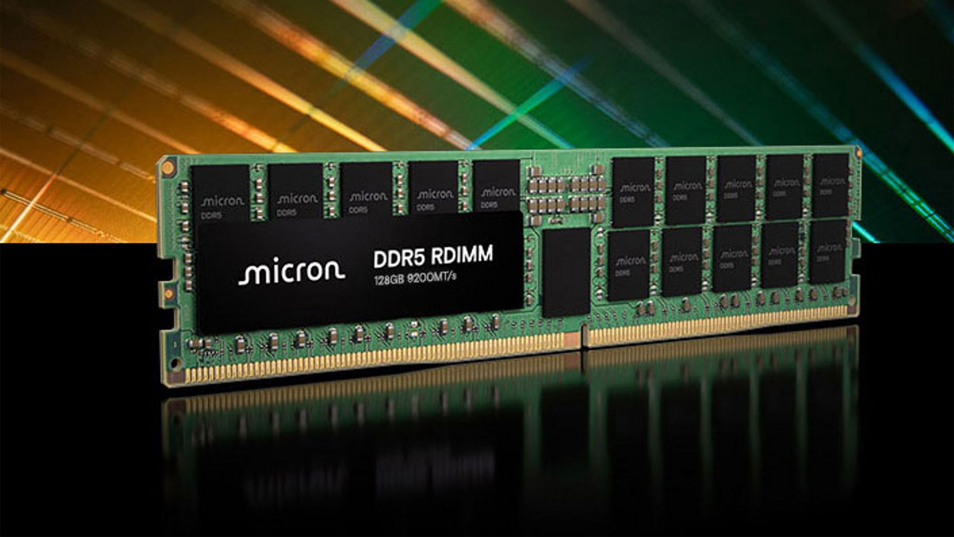
Last month, Micron disclosed its DRAM and NAND memory roadmaps for the next several years, revealing plans to use wafer bonding, new materials that enable making NAND cells smaller, High-NA EUV lithography, and detailing its moves toward 3D DRAM. Perhaps the most revealing part of Micron's story is that the company plans to expand its portfolio of custom DRAM and NAND products as AI developers increasingly require memory and storage solutions optimized for their unique processor architectures and specific workloads.

Micron

(Image credit: Micron)

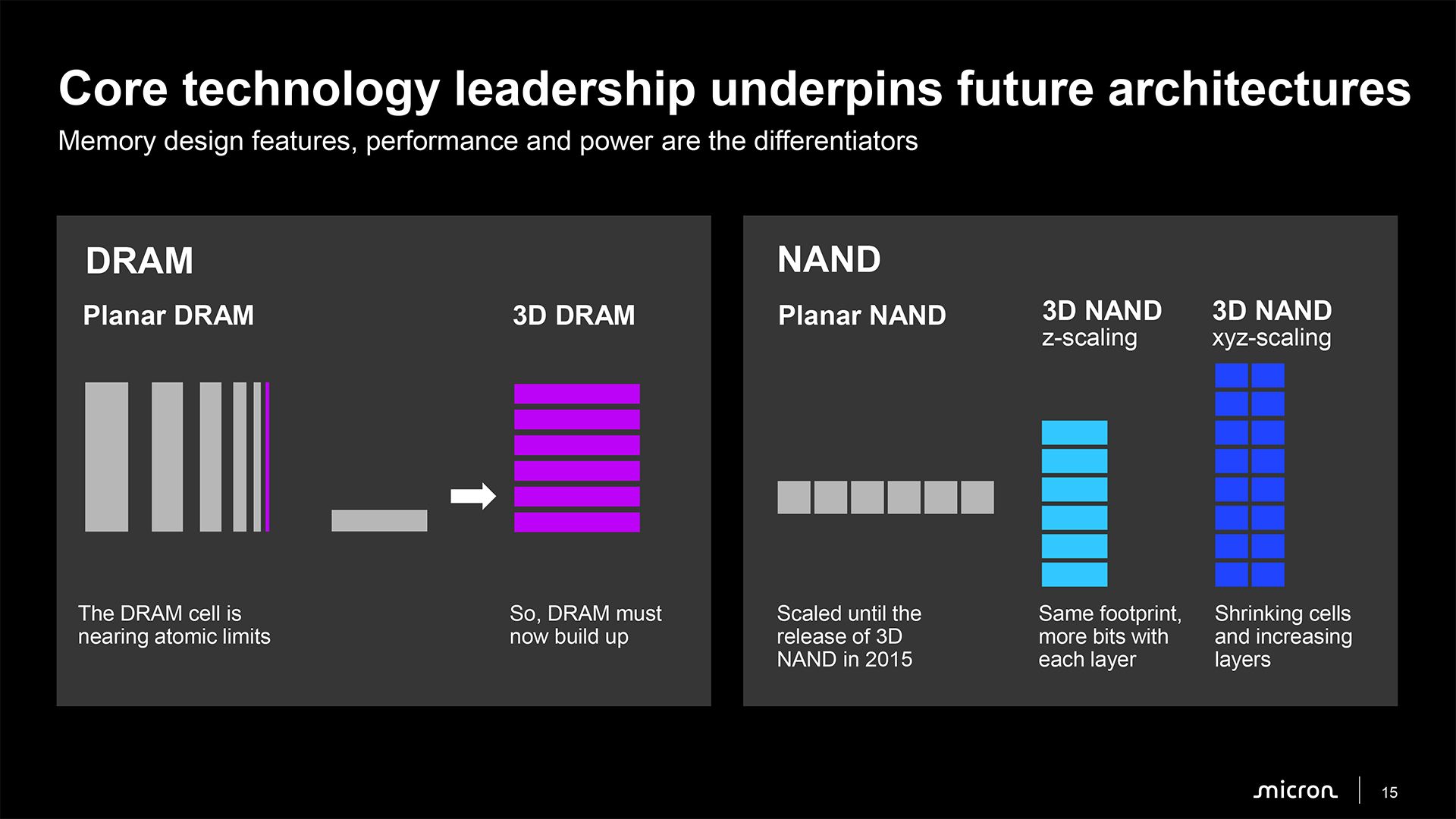
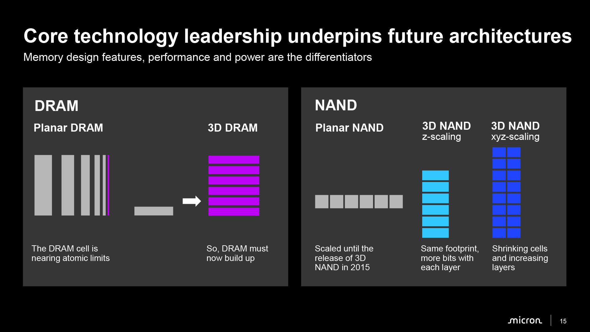
" DRAM is nearing atomic limits at this point: although we have confidence in several more planar nodes, we are very focused on making sure that we introduce 3D DRAM at the optimal time from a cost and performance point of view," said Scott DeBoer, president and chief technology and products officer at Micron, at the company's event earlier this month. "[With 3D NAND, we are] really focused on new materials densifying the cell architecture, and continuing to focus on that XYZ scaling going forward."

DRAM: 4F2 cells axed, High-NA EUV lithography, new materials, and 3D DRAM enable future scaling

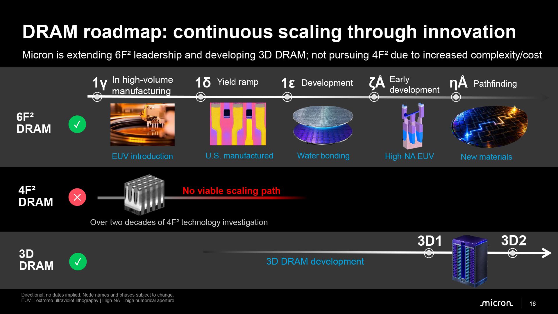
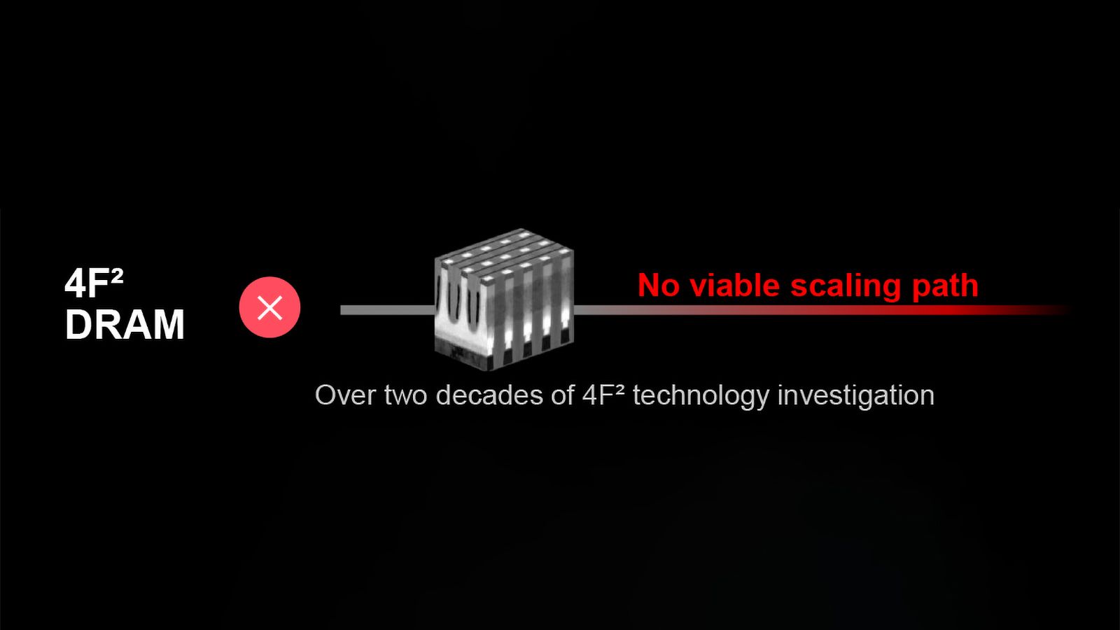
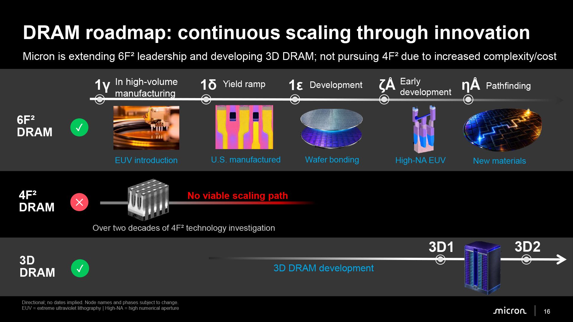
In a surprising move, Micron decided to abandon plans to produce DRAM with 4F2 memory cells, unlike its rivals at CXMT, Samsung, and SK hynix, citing the lack of a viable scaling path beyond where Micron is today. Instead, Micron's roadmap for the coming years includes wafer bonding, High-NA EUV lithography, new materials, and eventually 3D DRAM. The company plans to begin mass production of its next-generation 1δ memory in the second half of 2027, while subsequent 1ε, ζÅ, and ηÅ technologies are at various stages of development. In parallel, Micron is developing two generations of 3D DRAM that could eventually succeed conventional planar memory.
Micron

(Image credit: Micron)

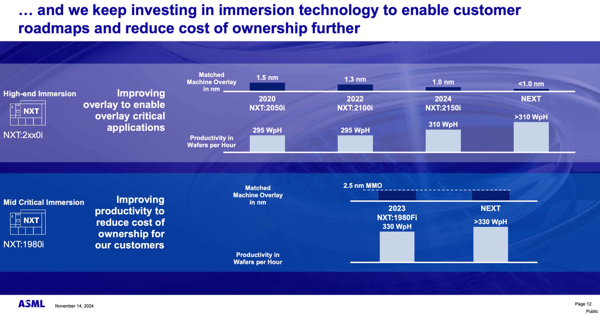
Micron's current 1γ (1-gamma) DRAM process technology, which is in high-volume manufacturing (HVM), is the company's first DRAM node to use EUV lithography. Previously, Micron had used multipatterning with DUV lithography and remained competitive with Samsung and SK hynix, which relied on EUV for critical layers.

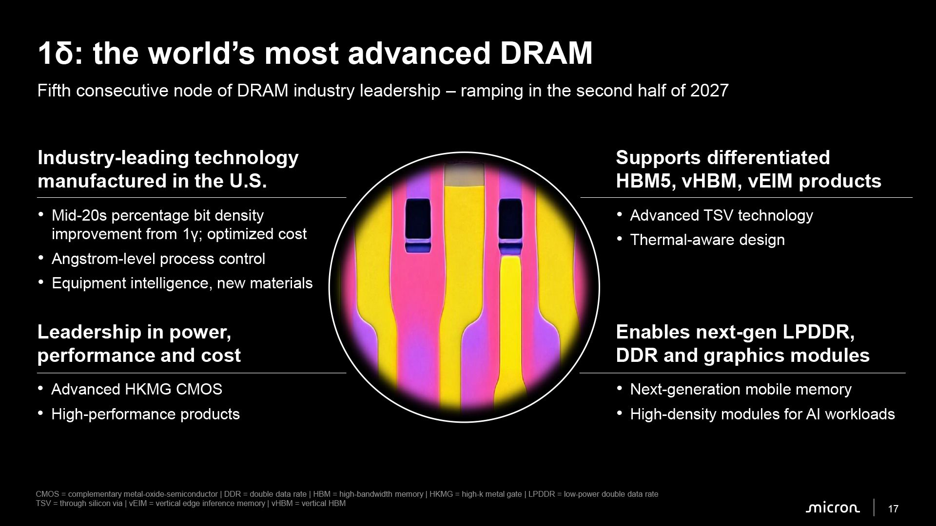
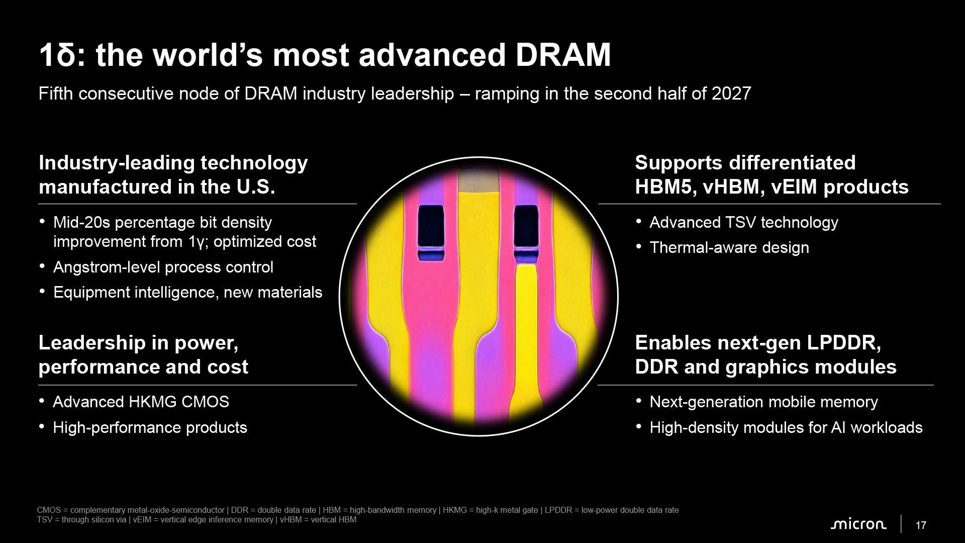
Micron's next-generation 1δ (1-delta) fabrication process is currently in the yield ramp stage and is scheduled to enter mass production in the second half of 2027. The company expects the technology to increase bit density by mid-20% compared to 1γ, while advanced high-k metal gate (HKMG) CMOS, new materials, angstrom-level process control, and equipment intelligence should improve performance, power efficiency, and ultimately yields as well as costs.
Micron

(Image credit: Micron)

Micron plans to manufacture 1δ DRAM in the U.S. and use the technology for next-generation DDR, LPDDR, graphics memory, HBM5, vertical HBM (vHBM), and vertical Edge Inference Memory (vEIM) products. Meanwhile, to make HBM5, vHBM5, and vEIM products, the node will also support additional features like through-silicon vias (TSVs) and other elements to improve thermal performance.

The subsequent 1ε (1-epsilon) process will rely on wafer bonding, which will enable Micron to produce different structures on separate wafers and then bond them together. This approach could increase flexibility in memory design and manufacturing, but Micron has yet to disclose its plans to implement wafer bonding, which structures it will bond, or what improvements in density, performance, and power consumption the technology will provide. The process is currently under development, and there is no announced production schedule.

Micron's ζÅ (zeta-angstrom) production node is currently in early development and will introduce High-NA EUV lithography to memory manufacturing, which will enable further reductions in critical dimensions. The company has not disclosed how many layers will require High-NA lithography, the expected density improvements, or when the technology will enter mass production. However, it is obvious that the node will not be here until at least 2030, years after Samsung and SK hynix adopt High-NA EUV at their DRAM fabs (planned for 2028).

The ηÅ (eta-angstrom) process represents the most distant generation on Micron’s disclosed planar DRAM roadmap and is currently in the pathfinding stage. After Micron inserts High-NA EUV lithography into its DRAM production flow, the company intends to bet on other methods of scaling. Although Micron mentions new materials, it hasn't identified them or explained how they will affect device structures. These could include new photoresists, deposition precursors, dielectric materials, or conductive materials that would enable the company to manufacture smaller transistors and capacitors, and ultimately increase DRAM cell density.

In any case, Micron's roadmap is focused on continuing development of DRAM based on 6F² cells, which differs from the plans of CXMT, Samsung, and SK hynix.

3D1 and 3D2: Transition to 3D DRAM is looming

In parallel with conventional DRAM development, Micron is working on two generations of 3D DRAM, currently called 3D1 and 3D2. Unlike planar DRAM, which primarily relies on smaller memory cells to increase bit density, 3D DRAM would use the vertical dimension to accommodate more memory cells within a given area. Micron intends to introduce the technology when it becomes competitive with conventional DRAM in terms of manufacturing costs and performance. The company has not disclosed architectures, layer counts, or density targets.

In fact, while Micron has outlined its future memory architectures through 2030, its DRAM manufacturing roadmap provides a firm production window only for the 1δ process, which is scheduled to enter high-volume manufacturing in the second half of 2027. The company has not disclosed production dates for subsequent planar DRAM nodes or either generation of 3D DRAM.

Custom HBM and vertical memory architectures

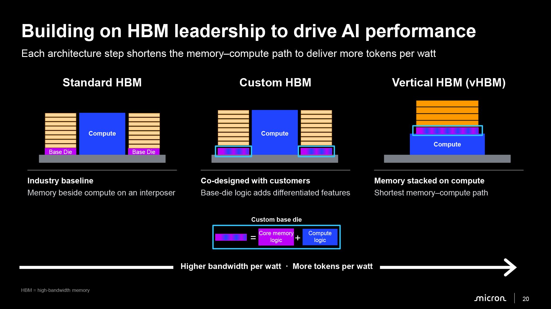
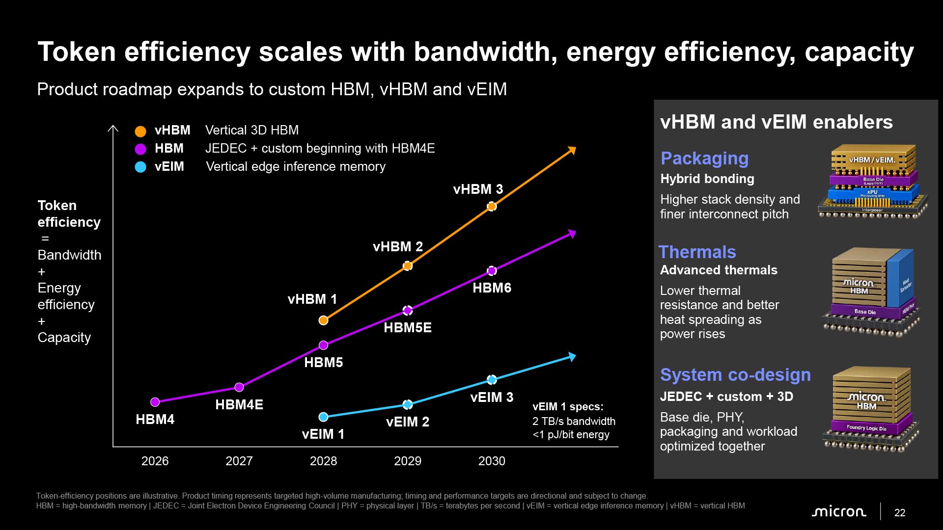
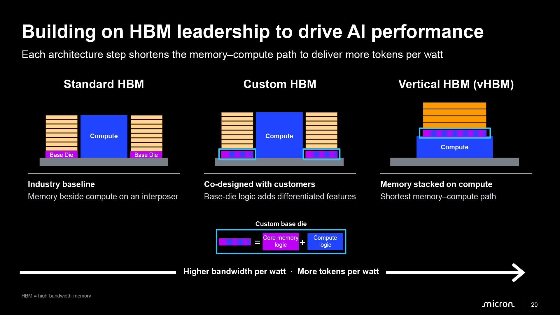
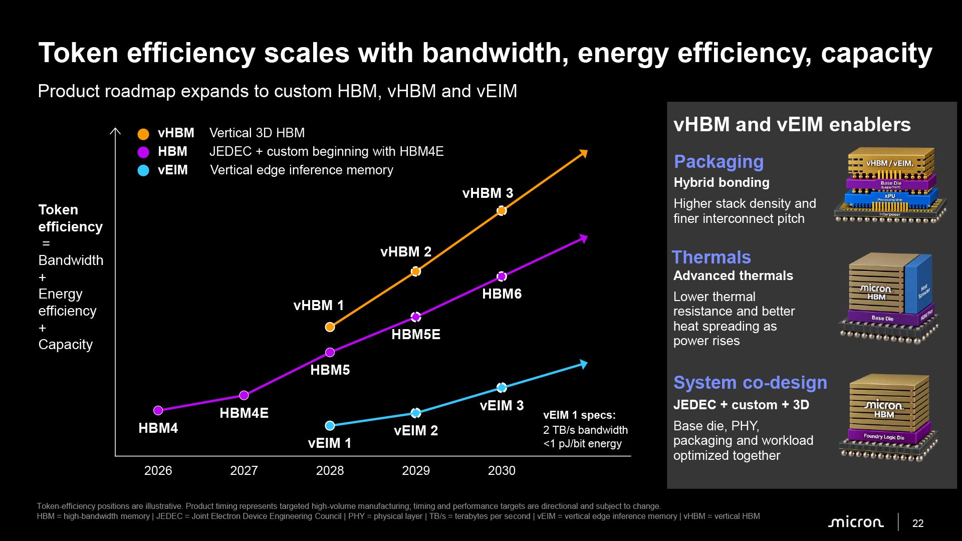
In addition to conventional DRAM, Micron plans to use its future manufacturing technologies for HBM4E, HBM5, HBM5E, and new vertically integrated memory architectures. Starting with HBM4E, the company will offer both standard and custom HBM products, which will be followed by custom HBM5E, vHBM, and vEIM (vertical Edge Inference Memory). All of these will mark the re-emergence of custom memory in mass-produced products.
Micron

(Image credit: Micron)

Custom HBM4E (cHBM4E) will enable Micron's customers to shrink memory I/O width and/or integrate additional logic into the memory's base die to free up valuable die space for compute and optimize performance and power consumption for specific AI accelerators. According to Scott DeBoer, Micron’s president and chief technology and products officer, some of these functions would otherwise reside in the ASIC itself, so moving them closer to memory should improve overall system efficiency.

"When we co-design a base die, and the certain logic elements that are desired to be put in that base die are generally an offload from GPU circuitry anyway onto the base die to put it closer to the memory," said DeBoer. "Moving what makes more sense onto the base die will still be a reality in [the] vertical HBM timeframe as well."

To support these capabilities, Micron intends to use advanced foundry process technologies for the base dies of both standard and custom HBM products, although it has not disclosed specific nodes. For custom designs, the company will select the most cost-effective process that meets customer requirements. For example, Micron expects HBM4E to require more advanced CMOS technologies to meet its performance and power targets.
Micron

(Image credit: Micron)

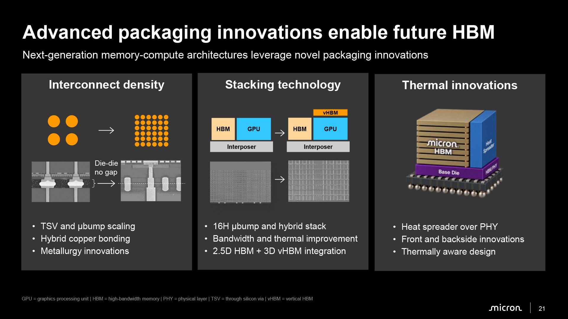
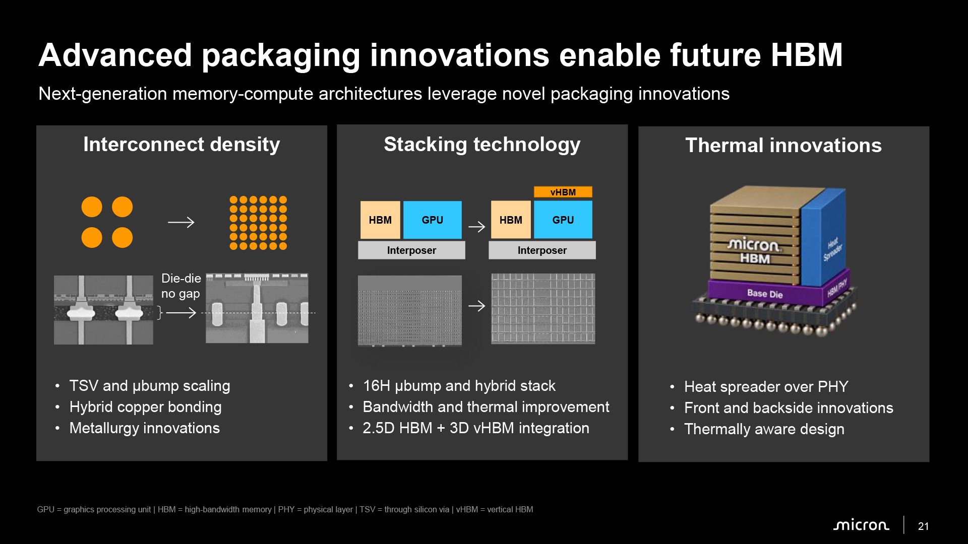
Further down the road, Micron intends to introduce vertical HBM (vHBM), which will stack memory directly on top of ASICs and CPUs rather than next to them on an interposer. This architecture promises substantially higher bandwidth, thanks to dense vertical connections (as well as significantly lower latencies) thanks to adjacent placement, but it is also set to create considerable challenges related to power delivery and heat dissipation. To address them, Micron plans to use hybrid bonding for advanced interconnects, integrated heat spreaders, and thermally aware designs. Interestingly, the company expects conventional HBM and vHBM to coexist in some designs, where vHBM provides maximum bandwidth, while traditional HBM serves capacity requirements.

Another technology under development is vertical Edge Inference Memory (vEIM), which shares many of its packaging and integration technologies with HBM, but targets applications that require power efficiency more than maximum bandwidth. Micron's 1st Generation vEIM aims to deliver formidable HBM4-like 2 TB/s of bandwidth while consuming less than 1 picojoule per bit of data transfer energy.

Both architectures will require close cooperation with customers to optimize memory, logic, packaging, and thermal characteristics for particular applications, so Micron will need to work with its clients to make vHBM and vEIM successful. Interestingly, Micron's customer-specific development efforts extend beyond HBM and EIM.
Micron

(Image credit: Micron)

For example, the company is collaborating with Meta to optimize LPDDR6 for data center applications, which primarily include reliability, serviceability, and availability. Micron expects LPDDR6 to reduce power consumption by approximately 35% compared to LPDDR5, which will be very important for dense memory deployments. The company also intends to develop DDR6 — which targets 2X DDR5 bandwidth — in cooperation with major customers to better understand and ultimately meet their needs.

Speaking of customer cooperation, DeBoer stresses that Micron now collaborates with customers from the earliest stages of product definition through joint design, development, validation, and volume production. According to the executive, this approach differs substantially from how the company worked with customers previously.

"Across our AI co-invention opportunities we are co-imagining, co-designing, co-developing, co-validating, and then delivering at scale," DeBoer said. "This opportunity is truly unique. It is very different than the way we interacted with customers even three or four years ago."

Advanced CMOS: More than 10X performance improvement

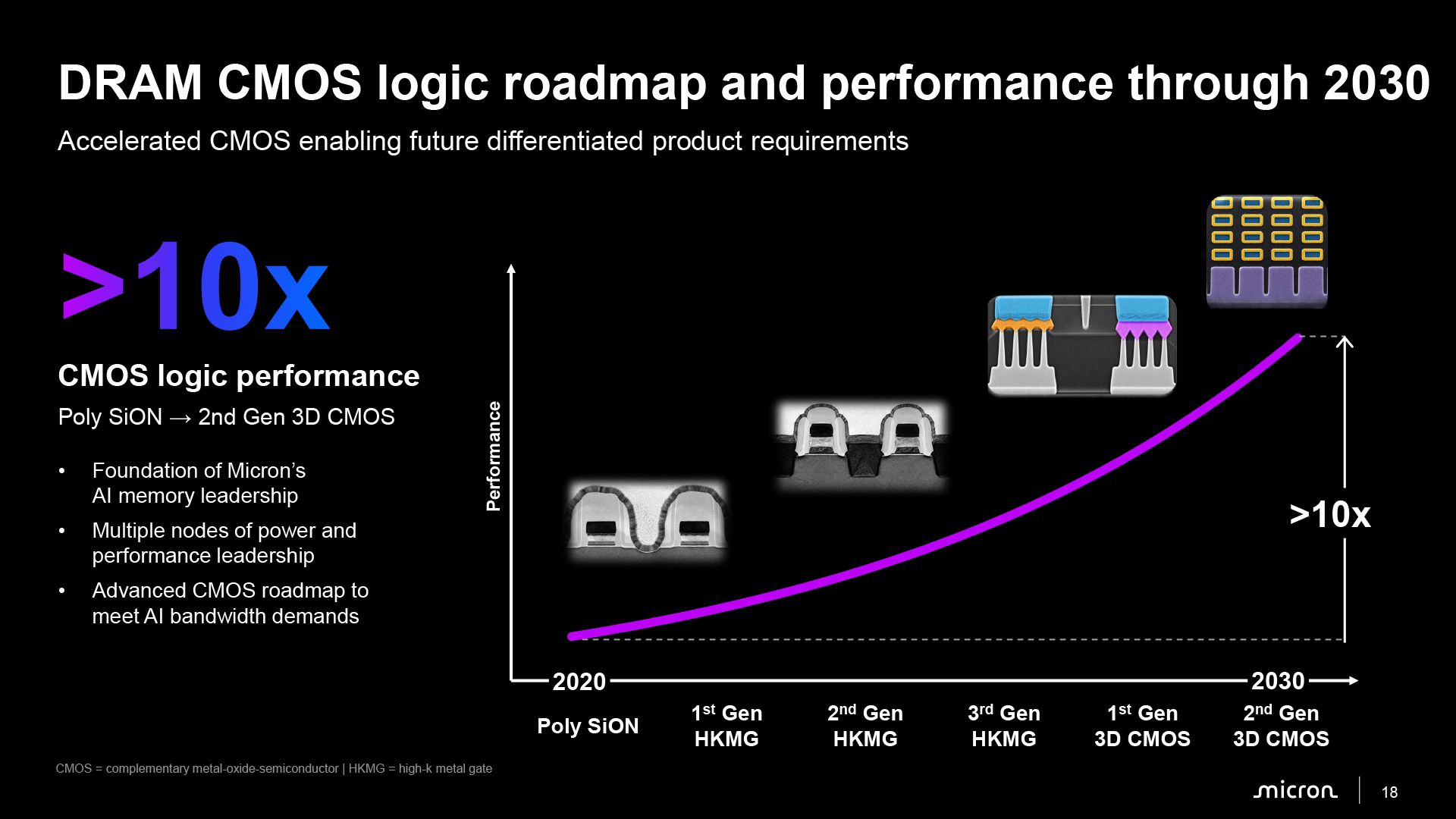
In addition to shrinking DRAM cells and developing vertical memory architectures, Micron is developing advanced CMOS technologies for peripheral circuitry. The company's roadmap includes several generations of DRAM CMOS logic with high-k metal gate transistors, followed by 1st and 2nd Generation 3D CMOS technologies.

Micron expects these advances to increase its CMOS logic performance by more than 10X between 2020 and 2030, which should help the company address the growing bandwidth and power requirements of AI-oriented memory products.

3D NAND: From next-gen 400L 3D NAND to AI-oriented NAND

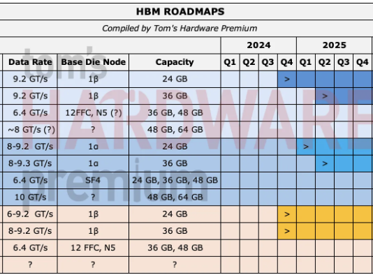
Although Micron's event was mostly dedicated to the future of DRAM, the company also shared some details about its upcoming NAND innovations, which include 11th Generation 3D NAND with 400 layers, post-G11 3D NAND, and AI-oriented NAND memory that either offers high bandwidth or high IOPS.

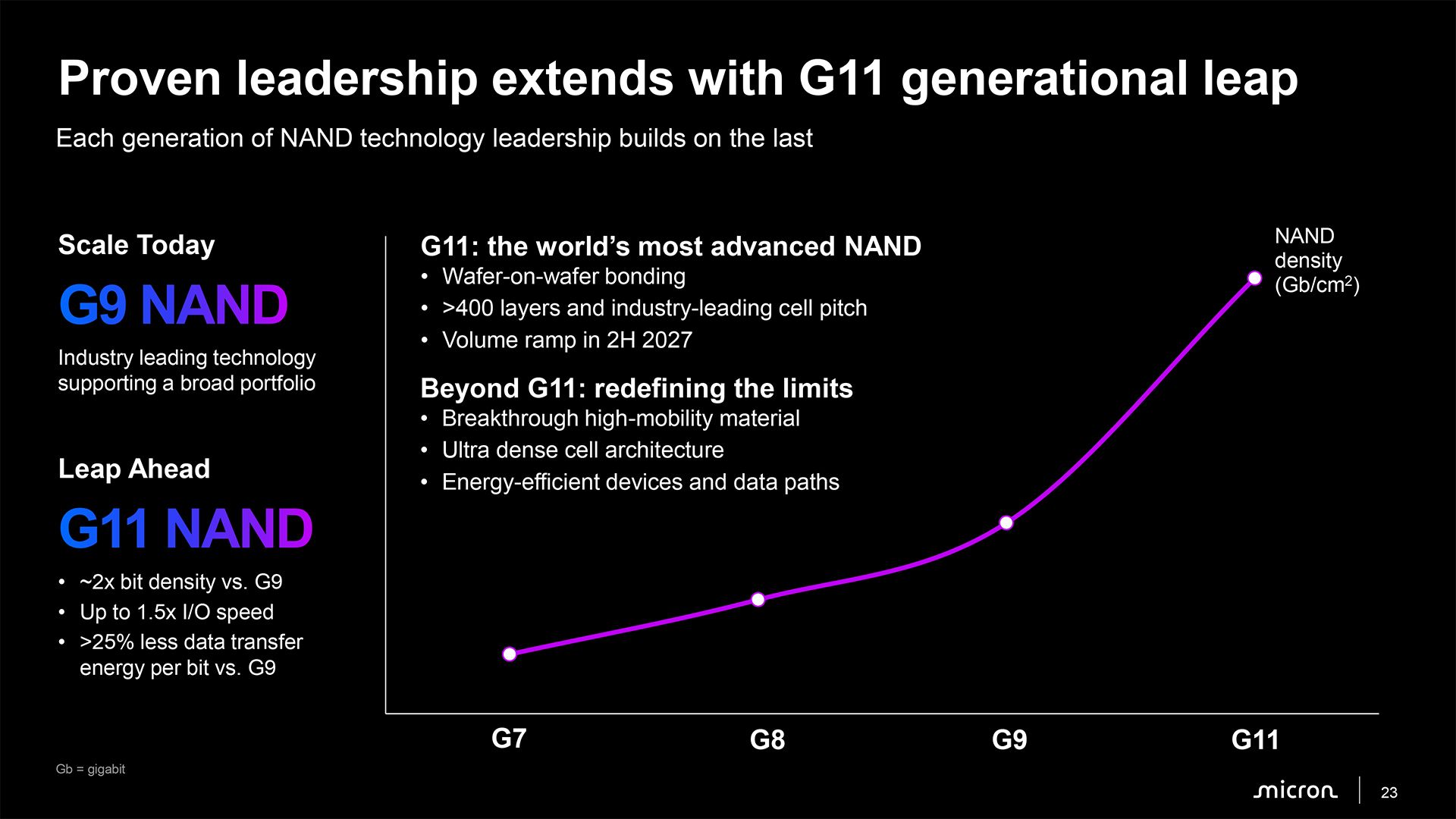
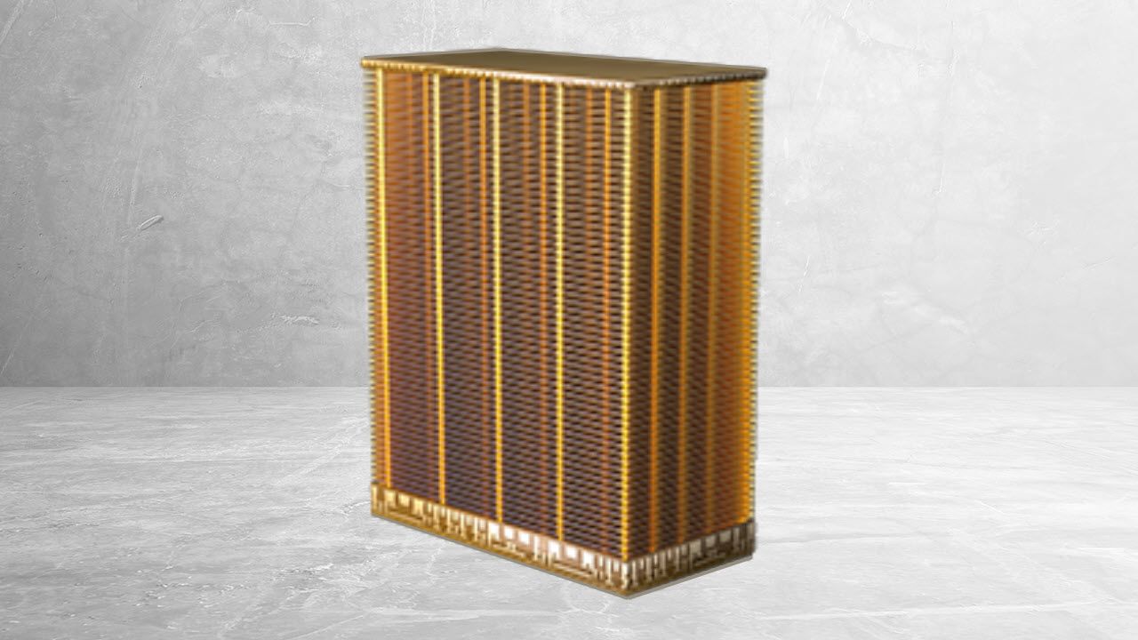
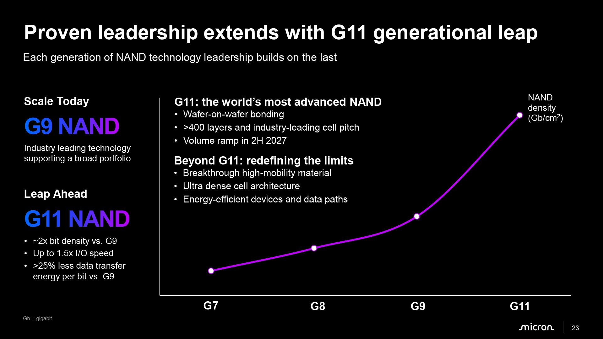
Micron's next-generation G11 (N170) 3D NAND technology represents a substantial departure from its current G9 (N160) process. The company plans to increase the number of active memory layers from 276 to more than 400, introduce wafer-on-wafer bonding, and implement an industry-leading memory cell pitch.

These improvements are expected to double the bit density of G11 3D NAND compared with G9 3D NAND, presumably from 21 Gb/mm2 to 42 Gb/mm2 in the case of 3D TLC devices, which should substantially reduce manufacturing costs per bit once the technology reaches mature yields.
Micron

(Image credit: Micron)

In addition to increased storage density, G11 also targets a 50% increase in I/O speed compared with G9, which implies a potential transfer rate of approximately 5,400 MT/s. Furthermore, Micron expects to reduce data transfer energy consumption by more than 25% per bit, an important improvement for high-capacity SSDs and AI storage systems that tend to move huge amounts of data.

One of the most important changes with G11 is the adoption of wafer-on-wafer bonding, which lets Micron manufacture memory arrays and the periphery and I/O circuits on another wafer, then bond them together. Chinese manufacturer YMTC has used this method to maximize storage capacity and performance, so it is not surprising that Micron and other memory manufacturers are adopting the technique as well.

Micron expects to start mass production of G11 3D NAND in the second half of 2027.

Improving 3D NAND past G11: New materials and further XYZ scaling

Micron intends to continue improving 3D NAND beyond 11th Generation through a combination of new materials, denser memory cell architectures, and more energy-efficient devices and data paths. Specifically, Micron is investigating high-mobility materials that could improve the electrical characteristics of future memory devices, as well as ultra-dense cell architectures intended to increase storage density beyond what an increase in active layers provides.

Meanwhile, more energy-efficient circuitry and data paths should help offset the growing power consumption associated with higher NAND capacities and faster interfaces.
Micron

(Image credit: Micron)

"Beyond G11, we have a strong roadmap, not going to go into great detail on it today, but really focused on new materials densifying the cell architecture, and continuing to focus on that XYZ scaling going forward," said DeBoer. "[…] The current industry direction and Micron’s direction is scaling both by adding layers [and] also by shrinking the cell dimensions."

The company has not identified the materials it intends to introduce or explained how they will affect memory cell structures. Nor has it provided quantitative density, performance, or power targets for NAND generations beyond G11.

AI-oriented NAND: Higher IOPS and bandwidth

Although Micron is not ready to share details about its G12 or G13 3D NAND generations, the company disclosed that it is developing two specialized NAND architectures for AI applications.

The first — High-IOPS AI NAND — architecture focuses on maximum random I/O performance and uses SLC-based designs with small blocks to accelerate workloads such as vector searches, graph analytics, and AI context management. Micron envisions products capable of delivering approximately 25 million to 100 million IOPS, depending on their configuration, and expects to bring products based on this approach to market over the next couple of years.

Micron

(Image credit: Micron)

The second — High-Bandwidth AI NAND — architecture prioritizes bandwidth over random I/O performance. Micron is investigating vertically stacked NAND devices connected through TSVs and equipped with a logic base die that resides close to AI accelerators, so from many points of view this concept resembles SanDisk's HBF. However, Micron does not believe that simply placing NAND stacks alongside AI accelerators on an interposer offers sufficient advantages. Instead, the company is exploring alternative integration approaches that bring NAND closer to compute resources, but don't necessarily consume valuable shoreline (the perimeter, or edge) of AI accelerators.

"[The High-Bandwidth AI NAND is] more costly and has to be implemented in partnership with customers in a way to ensure that they are meeting the mark and the cost point to drive the value proposition," DeBoer said. "We are enabling TSV-stacked NAND with a logic base die to bring memory closer to accelerators. We do not think placing it along the shoreline of the GPU has merit. Instead, we want to position it closer to the compute itself to take advantage of this high-performance NAND."

Micron

(Image credit: Micron)

These specialized AI-focused NAND architectures will complement Micron's conventional SSD roadmap, which includes plans for drives with capacities of up to 512 TB in the foreseeable future.

  •  

AMD expects to outsell Intel in Q4 for the first time in history

AMD late on Tuesday reported its highest quarterly revenue ever as demand for its Epyc data center processors and Instinct AI accelerators nearly doubled year-over year and sales of its products for client systems were down only modestly despite high memory prices and other headwinds.

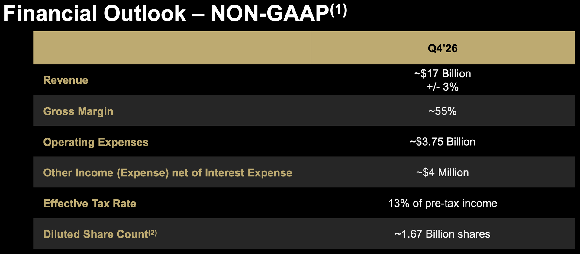
As increasing sales of data center hardware more than offset declines in the client realms, AMD's profitability continues to improve. Perhaps the most striking announcement AMD made is that it expects its Q4 revenue to reach approximately $17 billion, which would put it ahead of Intel for the first time in history.

AMD
AMD
AMD
AMD

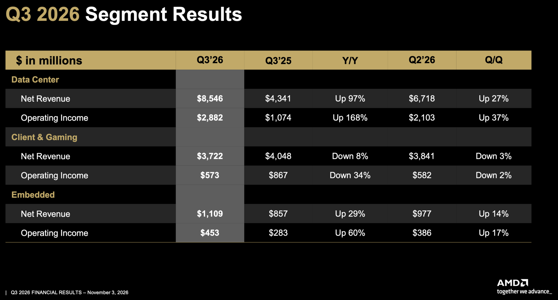
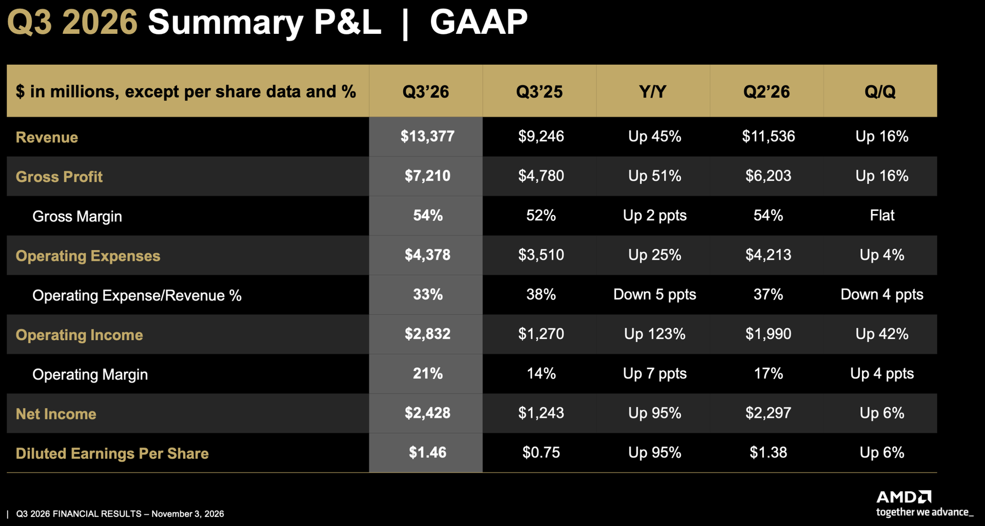
AMD's third-quarter revenue reached $13.377 billion, a huge increase from $9.25 billion in the same quarter a year earlier and $11.54 billion in the previous quarter. The company's gross margin was 54% during the quarter, and net income increased by 95% to $2.43 billion. Diluted earnings per share reached $1.46, compared with $0.75 in the same quarter last year.

Data center business now accounts for 64% of AMD's revenue

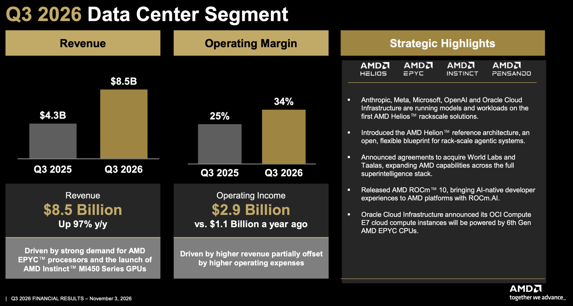
AMD's Data Center business was the main driver of its growth as the unit's sales reached a record $8.55 billion, up 97% from $4.34 billion a year earlier and 27% sequentially. The unit's operating income surged by 168% to $2.88 billion, while operating margin expanded from 25% to 34%.

AMD

(Image credit: AMD)

The company attributed the results to strong demand for its latest Epyc processors and the launch of Instinct MI455X AI accelerators, which power its Helios rack-scale systems. Specifically, AMD noted that Anthropic, Meta, Microsoft, OpenAI, and Oracle Cloud Infrastructure are already running workloads on their first Helios systems.

AMD expects its Data Center revenue to increase from $8.55 billion in Q3 2026 to approximately $12.8 billion in Q4 (based on the company's guidance), driven by the ramp of Instinct MI455X accelerators and Helios systems. The company also projects that its server CPU revenue will double in 2027, while Data Center AI accelerator and rack revenue will more than double, which will push the DC unit's contribution to over 80% of total company sales, up from 64% this past quarter and from 47% in Q3 2025.

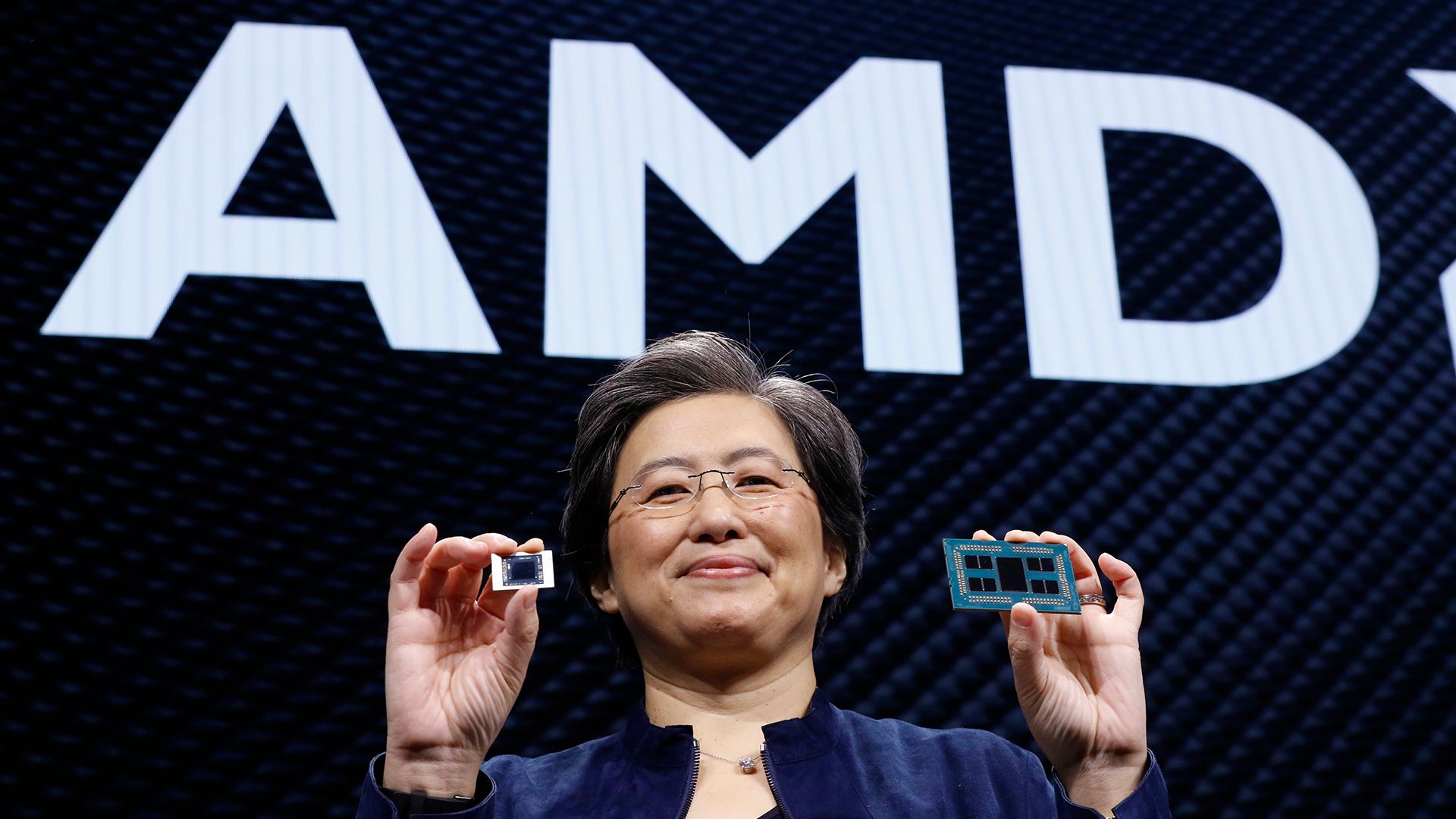
"We now expect server revenue to double year over year in 2027 and data center AI revenue to grow even faster than we projected ninety days ago," said Lisa Su, chief executive and chairman of AMD, during the company's earnings call with analysts and investors. "As a result, we expect data center to be more than eighty percent of our total revenue in 2027 and to drive the majority of our revenue and earnings growth."

Client revenue up, gaming revenue drops

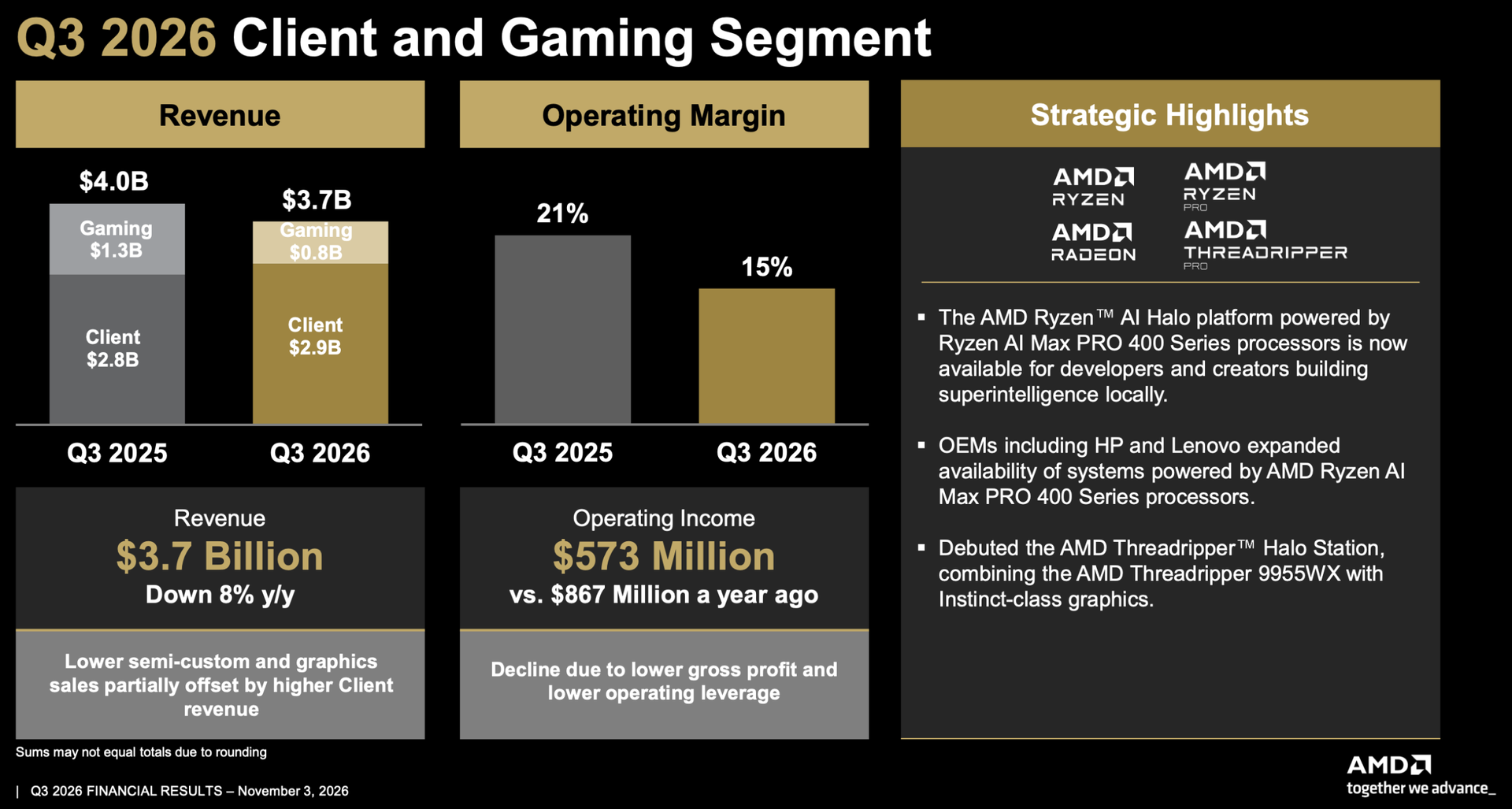
AMD's Client and Gaming business unit generated $3.722 billion in revenue, down 8% year-over-year and 3% quarter-over-quarter.

AMD

(Image credit: AMD)

Meanwhile, sales of AMD's client CPUs totaled $2.95 billion, down from $3.06 billion in the previous quarter and up around $200 million from $2.75 billion in the same quarter a year ago.

Sales of AMD's gaming products — including discrete GPUs and system-on-chips for game consoles — dropped to $773 million from $1.298 billion in the previous year as Microsoft and Sony bought fewer console SoCs, while sales of discrete Radeon RX GPUs remained weak during the quarter. The combined segment's operating income dropped by 34% to $573 million as the unit's operating margin decreased to 15%.

"In 2027, we are planning for PC market unit shipments to decline by a double-digit percentage," Su said. "In this environment, we expect to outperform the market as we deliver our rising roadmap and grow our commercial footprint."

AMD projects its Client and Gaming business to contract by more than 20% sequentially in Q4 2026 as higher memory prices weaken PC demand. The company is also preparing for a double-digit decline in PC shipments in 2027, although it expects to outperform the market by concentrating on enterprise, premium consumer, and desktop processors. Unfortunately, AMD did not provide a specific revenue forecast for its Client and Gaming segment for 2027.

Embedded business strong, set to accelerate

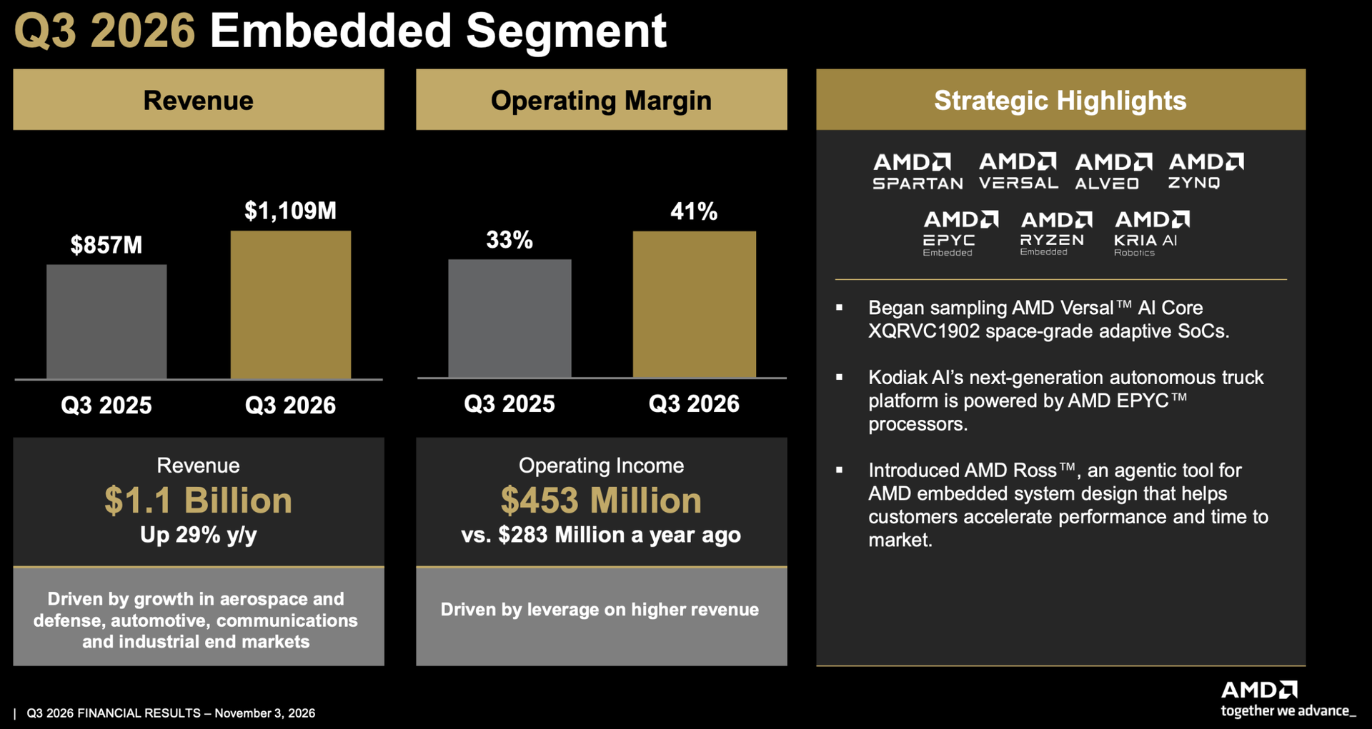
As for AMD's Embedded business, it also demonstrated strong growth as its revenue increased by 29% year-over-year to $1.11 billion and operating income rose by 60% to $453 million. The company attributed the improvement to stronger demand from aerospace and defense, automotive, communications, and industrial customers.

AMD

(Image credit: AMD)

AMD expects its Embedded business to grow by double digits sequentially in Q4 2026, then experience double-digit annual revenue growth over the next several years.

"Data center build-outs are also driving higher demand for our embedded CPUs and adaptive SoCs in control plane and optical networking applications," said the head of AMD. "We remain on track to close more than eighteen billion of design wins in 2026, our third consecutive record year."

Beating Intel

For those of our readers who have been following the CPU market in general as well as AMD and Intel in particular for decades, arguably the most earth-shattering part of AMD's earnings report is its outlook for the fourth quarter. The company expects revenue of approximately $17 billion, plus or minus 3%, which implies a 66% year-over-year increase and 27% sequential growth at the midpoint.

In contrast, Intel expects fourth-quarter revenue of $15 billion to $16 billion amid weakening PC demand and manufacturing capacity constraints.

AMD

(Image credit: AMD)

If AMD meets its guidance, its quarterly sales will surpass those of its considerably bigger rival Intel for the first time in history. In fact, AMD will not only leave Intel formally behond, but its projected advantage will be approximately $1.5 billion at the midpoint of both companies' forecasts, which is a tangible lead.

The development reflects the companies' increasingly different positions on the market: AMD is rapidly expanding its data center CPU and AI accelerator businesses, while Intel continues to depend heavily on PC and enterprise server processors, which sales face headwinds due to high memory prices and components shortages.

  •  

Intel 14A moves closer to production as PDK 0.9 becomes available

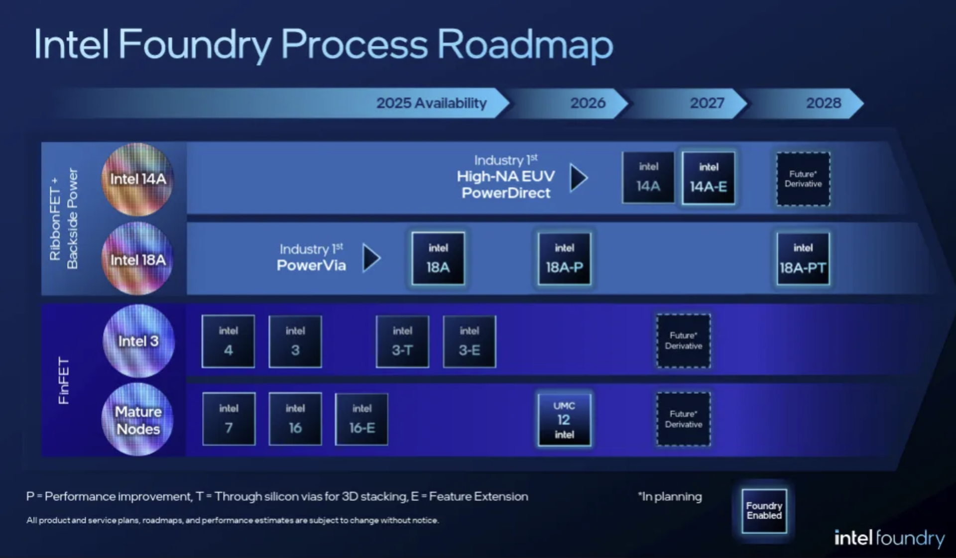
Intel Foundry last week made available its Intel 14A process design kit (PDK) version 0.9, an important milestone in the development of this next-generation manufacturing technology. The company says that the production node is reaching performance and yield maturity expected at this stage of development, and the results are backed by silicon validation. Intel plans to release PDK 1.0 in the first quarter of 2027, which will validate the technology's readiness for high-volume manufacturing (HVM).

14A PDK v0.9 is here

A process design kit contains transistor models, design rules, and other information that enables chip designers to develop products for a particular manufacturing process using electronic design automation (EDA) tools. The accuracy and quality of the PDK are crucial for modelling how chips will perform once manufactured, and the release of PDK 0.9 is particularly important because it provides customers with a representation of Intel 14A based on actual silicon measurements rather than on theoretical models or simulations. At this stage, customers can proceed with product development with greater confidence that the technology will meet their requirements when it comes to performance and power consumption.

Intel Foundry Roadmap

(Image credit: Intel/Tom's Hardware)

Intel says that PDK 0.9 lets customers develop designs intended to enter risk production around the time the process is certified, which — provided that PDK accurately reflects the characteristics of manufactured silicon — in many cases enables chip developers to greatly reduce the number of silicon revisions between initial tapeout and mass production. Of course, availability of PDK 0.9 does not indicate that Intel 14A is ready or even close to mass production, as the company expects to validate HVM readiness only with PDK 1.0, sometime in Q1 2027. Again, this does not mean that 14A will enter mass production in early 2027, as Intel itself expects to begin mass production using its 14A process technology in 2028, following risk production for its own products in the second half of 2027.

"From a customer perspective, the PDK 0.9 gives customers the confidence to design products on Intel 14A, as the technology is reaching the industry-standard performance and yield maturity expected at this stage of development, supported by silicon-backed validation," said Ben Sell, corporate vice president and general manager of front-end technology development at Intel Foundry.

Building on top of 18A

Intel 14A builds on top of architectural foundations introduced with Intel 18A but incorporates several substantial enhancements. These include 2nd Generation RibbonFET 2 gate-all-around (GAA) transistors, PowerDirect backside power delivery (which delivers power right to the transistor source/drain regions without using intermediate connections like TSVs used by PowerVia), and Turbo Cells (high-performance standard cells designed to accelerate timing-critical paths in CPUs and GPUs), which provide chip designers with additional ways to increase performance and optimize power efficiency. Since Intel has previously outlined advantages of these technologies, the latest announcement does not provide updates regarding transistor performance, power consumption, or transistor density figures for Intel 14A.

Beyond improvements to transistor, power delivery, and interconnect technologies, Intel is applying manufacturing experience gained during 12 months of Intel 18A production to accelerate maturation of 14A. Specifically, the company says it has increased investments in inline defect detection, modeling, and simulation to identify potential manufacturing problems earlier in the development cycle. These initiatives are intended to improve manufacturing yields, process variability, ultimately transistor performance, and reduce production cycle times. Intel also says it has introduced several strategic initiatives to accelerate technology development, although it does not quantify their impact.

New collaboration model

Another important change concerns Intel's relationships with equipment and materials suppliers. The company says it has revised its collaboration model to involve technology development teams and external suppliers earlier in the process development cycle. The goal of such close collaborations is to address manufacturing defects and improve equipment capabilities before they become obstacles for yield improvements after the technology enters mass production. Intel also conducts regular yield summit meetings with suppliers to accelerate progress on critical development objectives.

"This has required evolving our collaboration model with equipment and material suppliers, and earlier engagement from our [technology development] leaders with suppliers to drive improvements in defects and equipment capabilities," Sell said.

Intel

(Image credit: Intel)

A bonus of such early collaboration is that equipment and materials suppliers may incorporate Intel's requirements into their standard products and development roadmaps. This could give Intel an advantage over competitors, which would have to either adapt their manufacturing processes to equipment optimized around Intel's requirements or work with suppliers to develop alternative solutions from scratch.

Historically, Intel frequently set the direction for semiconductor manufacturing technologies as other chipmakers subsequently adopted similar approaches. One notable exception was immersion DUV lithography, which Intel adopted after TSMC, which led the development of immersion DUV lithography. By engaging equipment and materials suppliers earlier, Intel could regain some of its historical influence over the development of industry-standard manufacturing solutions, though the importance of this should not be overestimated.

Expanding design ecosystem

Meanwhile, Intel continues to expand the design ecosystem for its 14A technology. Cadence and Intel have established a design-technology co-optimization (DTCO) collaboration focused on next-generation AI-driven design tools and intellectual property, whereas Keysight, Siemens, and Synopsys have announced design-tool certifications for the process. Intel is also working with other software developers and IP providers to validate design flows and reusable building blocks required by prospective foundry customers.

Intel

(Image credit: Intel)

Intel says it is encouraged by customer feedback regarding the progress of 14A development. However, the company has not identified any customers that have committed to manufacturing products using the technology, disclosed customer tape-outs, or announced specific manufacturing agreements, which is normal for the foundry industry. For Intel Foundry, attracting external customers remains particularly important because development costs of modern leading-edge process technologies can only be recoupled when they are used to make hundreds of millions of chips, way more than Intel sells these days. Meanwhile, the commercial success of Intel Foundry with advanced manufacturing technologies depends not only on transistor performance and manufacturing yields, but also on its ability to deliver predictable development schedules.

Looking ahead, Intel intends to continue improving performance, yields, variability, and manufacturing cycle times of 14A, though for now the company does not disclose any actual goals. Intel also plans additional process enhancements and performance refinements for 14A-E and 14A-P nodes after the initial technology becomes available. However, exact schedules for these nodes are not known at the moment.

"Our next major milestone is the Intel 14A PDK 1.0, expected in the first quarter of 2027," said Ali Farhang, corporate vice president and general manager of Intel Foundry's design technology platform organization. "I am looking forward to sustaining this level of quality across future releases and continuing to earn our customers' trust by delivering on our commitments with a customer-first mindset."

  •  

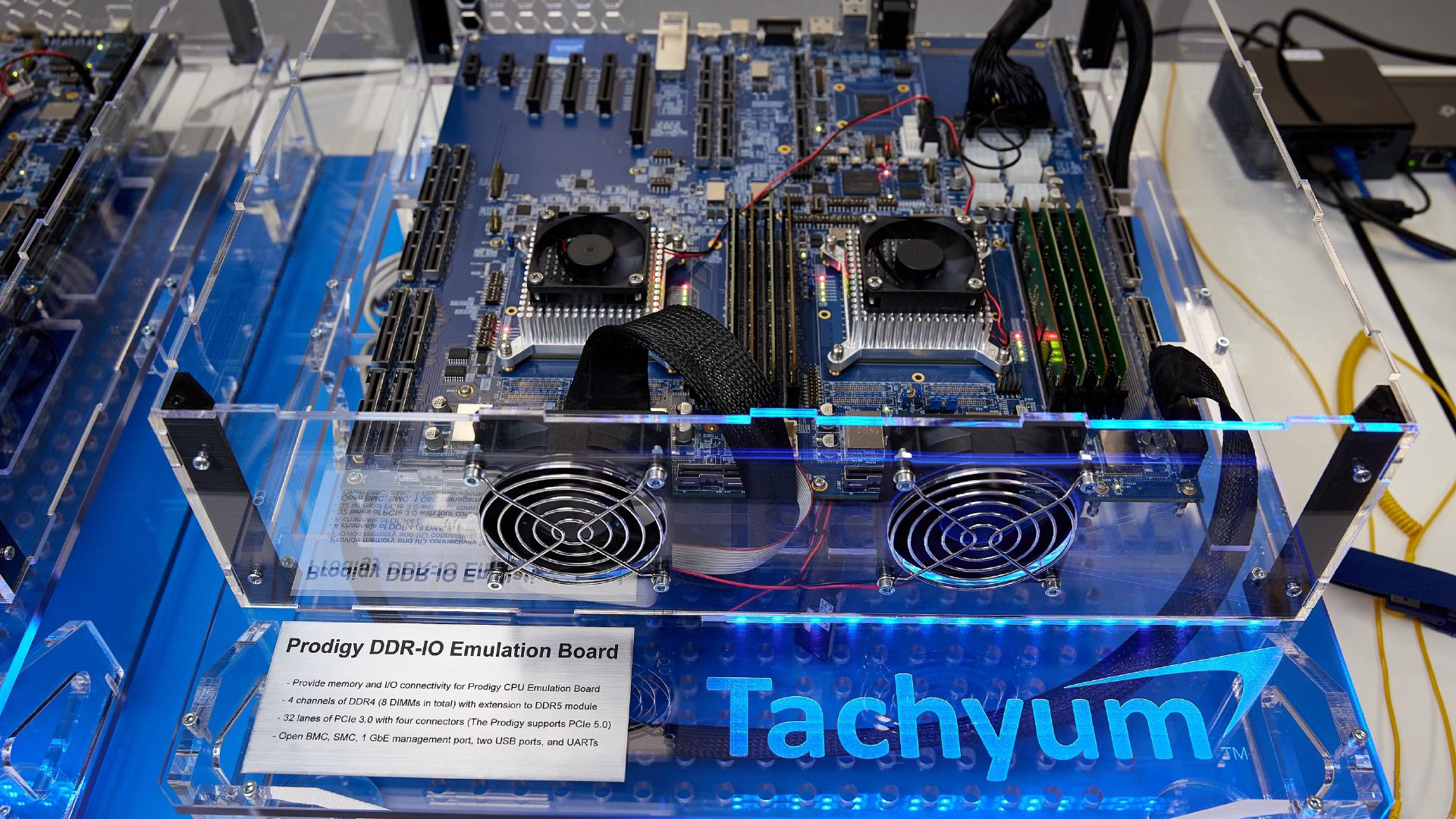
Tachyum, developer of heavily-delayed universal Prodigy processor, voluntarily files for bankruptcy

Tachyum, the company behind the overpromised and overhyped universal Prodigy processor, has filed for bankruptcy in Bratislava, Slovakia, reports Forbes (as observed by @System360Cheese). The filing follows a court order initiating bankruptcy proceeding after the company repeatedly missed its development and production milestones — but there are still theoretical chances that development of the processor will continue.

Despite eight years of development and numerous promises, Tachyum has yet to demonstrate working Prodigy silicon. Tachyum introduced Prodigy in 2018, targeting a 2019 tape-out and 2020 commercial availability. But the company repeatedly postponed the processor's launch, first to 2021, then to 2022, 2023, 2024, and eventually 2025.

Meanwhile, Prodigy's specifications changed considerably along the line: The original 64-core design evolved into a 128-core processor manufactured on a 5nm-class process technology, then a 192-core chip with 16 DDR5 memory channels. In late 2025, Tachyum announced yet another radical redesign: a chiplet-based architecture with 1,024 cores, 24 DDR5 memory channels, and TDP of 1,600W manufactured using TSMC's 2nm-class node. The redesign would require substantial additional development work and would have delayed commercial availability until 2030 or beyond.

According to court documents cited by Forbes, Tachyum Slovakia itself filed for bankruptcy on October 22, 2026, without waiting for a petition from creditors seeking to recover unpaid debts. The Bratislava III Municipal Court subsequently initiated bankruptcy proceedings after determining that the company's petition met the legal requirements. Under Slovak law, a company that voluntarily files for bankruptcy is presumed insolvent, according to Forbes, so technically Tachyum Slovakia is bankrupt.

If the court formally declares Tachyum bankrupt, a court-appointed trustee will take control of the company's assets, which could then be sold to repay creditors. We do not know at this point what these assets are, but theoretically they may include intellectual property related to its Prodigy processor, patents, and other technologies in addition to hardware used for development. Unless Tachyum secures additional financing or finds a buyer that can fund further development, work on Prodigy could effectively end.

Bankruptcy proceedings against Tachyum's Slovak entity do not necessarily mean that its affiliated companies elsewhere will also cease operations. Furthermore, the company's IP could survive under new ownership (if the company finds a buyer, or transfers IP ownership to another entity), which could theoretically let Prodigy development to continue. Nevertheless, the bankruptcy filing casts serious doubt on Tachyum's ability or intention to bring its long-delayed processor to market.

Theoretically, Tachyum's owners could potentially use bankruptcy proceedings to shed the company's debts, acquire its intellectual property through another legal entity, and resume Prodigy development. There are other options too.

Although most of Tachyum development activities are concentrated in Slovakia, Tachyum Slovakia is a subsidiary of the U.S.-based Tachyum Inc. according to Dennik N. If the American parent company owns the Prodigy IP, while the Slovak subsidiary employs engineers, conducts development, and accumulates debts, bankruptcy could enable the group to eliminate a substantial portion of those liabilities without losing its most valuable technological assets. In short, Tachyum's Slovak subsidiary could disappear along with much of its unpaid debt, while the American parent retains Prodigy IP and attempts to commercialize it somehow in the future. If the Slovak subsidiary owns the IP, the American parent could theoretically buy it from the bankruptcy estate and attempt to commercialize it eventually. Meanwhile, there is another complication: The American parent has reportedly faced pressure from its own creditors, some of whom have requested its liquidation, according to Dennik N. In this case, the destiny of the Prodigy IP is completely unclear.

For now, the future of Prodigy may depend on who actually owns Prodigy's intellectual property — Tachyum Inc. in the U.S. or Tachyum Slovakia — and whether the American subsidiary continues to exist or gets liquidated. The answer could determine whether this bankruptcy represents the end of Prodigy or a restructuring of the Tachyum group with the aim to continue development.

  •  

Intel shifts production capacity from consumer to server CPUs in face of 'unprecedented' AI demand

Although the consumer PC market is shrinking and will continue to shrink in the coming quarters, Intel is confident that the overwhelming demand from the AI industry for everything that can compute or store data will offset declines in the client space. To that end, the company is reallocating some of its capacity from client to data center CPUs, expanding its Fab 24 in Ireland to make more Xeons, has begun equipment installation into Fab 62 in Arizona ahead of schedule and vows to make 18A chips there, and is expanding its advanced packaging capacity in New Mexico and Malaysia.

"The industry continues to navigate one of the most significant supply shortages in history, driven by the unprecedented demand for Super Intelligence," said Lip-Bu Tan, chief executive of Intel, during the company's earnings call. "Against this backdrop, I am pleased by the progress we made growing our server supply in Q3. I am mindful about the ongoing challenges we face in the future quarters to keep pace with server demand."

More Intel 3-based Xeons

Intel's manufacturing expansion comes as demand for server processors continues to exceed supply despite substantial production increases over the next several quarters. The company's Data Center and AI (DCAI) business generated $7.3 billion in revenue in the third quarter of 2026, up 17% sequentially and nearly 80% year-over-year. Intel expects demand for data center CPUs to remain strong in 2027 – 2028 as AI infrastructure operators deploy more CPU-intensive agentic and inference workloads.

To meet demand for Xeon CPUs in the coming years, one of Intel's immediate priorities is to increase output of Xeon 6 'Granite Rapids' processors, which are made using its Intel 3 process technology. The company recently began expanding production capacity at its Fab 24 manufacturing complex near Leixlip, Ireland, but this capacity will only come online by the end of 2027, unless the move can be accelerated.

To further increase its Intel 3 capacity, Intel plans to convert some manufacturing resources at its Oregon facilities from Intel 18A to Intel 3. These resources were originally intended to manufacture Panther Lake client processors, but weaker PC demand has allowed Intel to prioritize higher-demand data center products. The company expects the additional Intel 3 capacity in Oregon to enter production in the second half of 2027.

"What we are taking offline to put Intel 3 into Oregon is 18A wafers, which we are generally going to build Panther Lake products," said Dave Zinsner, chief financial officer of Intel. "We see the opportunity with some of that capacity freed up to go produce more data center wafers."

Granite Rapids has already become Intel's fastest ramping server processor family, but demand continues to exceed available supply, according to the company's management. Intel is also improving manufacturing yields and reducing production cycle times to extract more usable processors from its existing capacity. According to the company, Intel 3 manufacturing costs have declined by approximately 15% since the first quarter of 2026.

Prepping for Diamond Rapids, Nova Lake

Intel is also accelerating the expansion of its leading-edge manufacturing operations in Arizona. The company is ramping Intel 18A production at Fab 52 and is accelerating equipment installation into the adjacent Fab 62, which is set to become the company's second high-volume manufacturing facility for 18A, 18A-P, and derivative process technologies.

These investments will support future Intel 18A/18A-P-based products, including server CPUs, although the company has not disclosed the precise allocation of manufacturing capacity between client and data center products at the facility. While the latter is natural, Intel said during the conference call that it expects to win some market share in the client space with its Core Ultra 400-series 'Nova Lake' CPUs, which will require the company to produce these parts in high volumes.

To support its capacity expansion, Intel aggressively procured new tools in the third quarter.

Not only wafers

While expanding production of Intel 3 and Intel 18A/18A-P wafers is a must to increase output of data center CPUs, producing more wafers will not necessarily solve Intel's supply problems. The company also faces shortages of advanced organic substrates required to package its multi-chiplet processors (or rather system-in-packages, or SiPs?) that rely on EMIB and/or Foveros 3D packaging technologies. Intel has been working with substrate suppliers to expand their production capacity and expects approximately 40% additional substrate capacity to become available in the second half of 2027.

"We are not only constrained on the wafer side, we are also constrained on the substrate side," Zinsner said. "So, it is important we get the substrate piece of this ramped up to be able to meet the demand."

In addition, Intel is expanding its advanced packaging operations in New Mexico and Malaysia to support growing demand from internal product groups and external customers. The company already uses its EMIB technology to connect multiple compute dies in Granite Rapids processors, while its newer Clearwater Forest Xeons combine EMIB with Foveros Direct 3D and hybrid bonding to stack Intel 18A compute dies on Intel 3 base dies. Additional packaging capacity will be essential as Intel increases production of these processors and introduces more complex multi-die products as well as assembles advanced system-in-packages using EMIB, EMIB-T, Foveros 3D, and other technologies for external clients.

"On Advanced Packaging, we are pleased by the progress we are making with EMIB and EMIB-T for our internal products," Tan said. "Both continue to see significant external customer traction as well. We continue to improve on execution, working with our supply chain to secure the capacity to meet the needs of our Advanced Packaging customers. We are also seeing robust progress in the readiness of Hybrid Bonding Interconnect (HBI), which is an enabler of 3D chip stacking for our upcoming server products."

Capital needed

Intel's expansions will require substantial capital. Intel expects its capital expenditure (CapEx) budget to reach approximately $20 billion in 2026 and increase significantly in 2027 (though it did not reveal any firm numbers). The company said firm purchase orders to semiconductor equipment suppliers increased by nearly 40% sequentially as it secured tools for its manufacturing expansion. Intel is also evaluating opportunities to accelerate construction of its semiconductor manufacturing complex in Ohio, where the first major structural truss was recently installed.

"We have made good progress securing the equipment required to support our growth plans with firm purchase orders to equipment suppliers increasing nearly 40% sequentially," Zinsner said. "We are also accelerating clean room build-outs, including Fab 62 in Arizona and exploring opportunities to accelerate in Ohio.

Yet Intel's capacity expansion will take time to produce results. New equipment must be installed and qualified, additional wafers must pass through lengthy manufacturing cycles, and substrate suppliers must increase their output (which will likely require them to procure new tools and install them) before Intel can ship more finished processors. Consequently, the company expects supply constraints to remain particularly severe during the first half of 2027, even as the client PC market is set to continue contracting.

Nevertheless, Intel expects its data center business to continue growing and believes that additional manufacturing capacity, higher yields, and improved substrate availability will enable it to capitalize on demand for AI infrastructure in the second half of 2027 and beyond.

  •  

Intel’s woes wipe out $1 trillion of semiconductor market cap in one day

Intel's shares plunged 30% on Friday, wiping out nearly $150 billion in market capitalization in a single day, the largest single-day loss in the company's history. The decline followed a disappointing financial outlook, largely driven by an anticipated drop of more than 20% in sales at Intel's client computing group (CCPG), the company's main cash cow. The declines quickly spread across the semiconductor industry. Although losses elsewhere were nowhere near as severe as Intel's, approximately $1 trillion in semiconductor market capitalization was wiped out on Friday, according to intraday estimates by Benzinga.

Fire sale

The PHLX Semiconductor Sector Index (SOX), which tracks the stock performance of 30 major semiconductor companies, is one of the key indicators of the industry's financial health. On Friday, the index plunged 9.14%, or 1,052.82 points, to 10,465.38 points as of 2:31 PM ET, as Intel's disappointing outlook triggered a massive selloff across the semiconductor industry.

Intel was by far the biggest loser, as other chip-related stocks, while Arm (-12.68%), AMD (-12.48%), Qualcomm (-12.14%), Applied Materials (-8.73%), ASML (-8.13%), Lam Research (-8%), Micron (-7.28%), and Broadcom (-7.1%) suffered considerably less. Then again, while Nvidia lost 5.66% of its market cap, this translates to around $270 billion, which is a massive amount of money. Paradoxically, Nvidia lost more market capitalization in absolute dollar terms than Intel.

In an unexpected turn of events, the downturn extended to server manufacturers and cloud giants too, as Dell (-12.67%), HPE (-8.10%), Supermicro (-6.96%), and Oracle (-6.88%) lost nearly 7% to 13% of their value. Reuters noted that investors increasingly question the scale of capital investments required to expand AI infrastructure as well as the sustainability of that spending.

Gloomy outlook

Intel’s client computing and physical AI group (CCPG) generated $8.1 billion in revenue during Q3 2026, down 5% year-over-year and 9% sequentially. Weaker demand and increased competition reduced client processor shipments by 14% year-over-year, which was partially offset by a 9% increase in average selling prices. CCPG accounted for nearly half of Intel's revenue of around $16.5 billion and the company's main source of cash. As strong demand for server processors only partially offsets declining client sales, Intel guided its Q4 revenue to be between $15 billion and $16 billion.

Intel expects the client market to deteriorate further in Q4 2026 and into 2027 as elevated memory prices and shortages of other components impact PC prices and demand. In general, Intel expects the client PC market to decline 10% in 2027 compared to 2026, which will inevitably have an effect on CCPG performance. While Intel expects its data center business to continue growing in 2027, industry-wide supply constraints will limit its ability to fully capitalize on demand.

2026 has been a mixed bag for Intel so far. On the one hand, the company achieved its highest market capitalization ever — $673.43 billion in mid-June — on growing sales of data center CPUs, strong sales of client products, and a return to profitability (if the $12.5 billion non-cash accounting charge associated with shares issued to the U.S. government is excluded). On the other hand, the company's capitalization has dropped by nearly 50% to $338.91 billion since mid-June (with $148.68 billion in just one day), as investors began to realize that the performance of Intel's CCPG heavily depends on memory prices, as customers and businesses tend not to like overpriced systems. Yet on the other hand, now that Intel sells fewer client processors, it can sell more expensive data center CPUs.

What about Apple?

Surprisingly, Apple (-1.66%), which only sells client products, was nearly unaffected by the performance of Intel's client computing group, as investors probably believe that the world's largest supplier of consumer electronics is more immune to memory prices than Intel. Ironically, if we count the A-series SoCs used in iPhones (which tend to outperform mainstream laptop CPUs), Apple sells substantially more processors than Intel, making Apple by far the world's largest supplier of microprocessors. Despite this, Apple's shares were largely unaffected by the semiconductor selloff.

There are several reasons for this distinction. Firstly, Apple's business model is fundamentally different. Intel sells processors to PC manufacturers, whereas Apple designs its own processors and sells them as part of finished products. Consequently, Apple captures revenue from the entire device rather than just the processor. Secondly, the two companies face different demand dynamics. Intel depends heavily on the PC market, while Apple's iPhone business follows the smartphone replacement cycle. Rising memory prices could affect both, but not necessarily to the same extent and at the same time.

There is an additional irony: Apple is also a major customer of TSMC, so its processor supply chain overlaps with those of AMD, Intel, and other semiconductor companies whose shares declined sharply.

While we should not directly compare Apple and Intel, the comparison illustrates that investors were not necessarily abandoning companies that design or use semiconductors, but were rather concerned about the profitability and growth prospects of these high-tech companies. And if we take a look at the situation from this point of view, the whole thing will start looking completely different.

  •  

Deadly Intel Fab 28 explosion causes two-week shutdown, to cost $600 million and severely disrupt server chip manufacturing for six months

The explosion at Intel's Fab 28 near Kiryat Gat, Israel, that happened earlier this month forced Intel to shut down the whole facility for two weeks, and now the company expects that it will cost it approximately $600 million in lost revenue over two quarters. The disruption is expected to affect server processors manufactured using Intel's 10nm-class process technologies and will reduce the company's shipments in both the fourth quarter of 2026 and the first quarter of 2027.

"In Israel, we have been shut down for about two weeks," said Dave Zinsner, chief financial officer of Intel, during the company's earnings call. "We feel like we are going to be starting up production here by the end of this week."

The explosion occurred in mid-October, killed two, seriously injured one, and caused an extended shutdown of Fab 28, one of Intel's key manufacturing facilities for chips produced using its 10nm-class and Intel 7 process technologies (Intel 7 was formerly called 10nm Enhanced SuperFin). Intel expects the incident to reduce its Q4 2026 revenue by approximately $300 million, and a similar impact is anticipated in Q1 2027. The company also expects the accident to reduce its fourth-quarter non-GAAP gross margin by approximately 2%.

Intel has not identified the affected Xeon processor families, disclosed the number of wafers damaged, or specified when Fab 28 will return to full production capacity after it restarts this Friday.

Although Intel's latest Xeon 6 processors use compute dies produced on Intel 3 fabrication technology, they still use I/O dies fabricated on Intel 7 (aka 10nm ESF) fabrication process. Furthermore, Intel continues to sell previous-generation Xeon 5 Emerald Rapids (and even Xeon 4 'Sapphire Rapids', though it stopped accepting orders on these CPUs in late September) that are made on Intel 7 manufacturing technology.

While Intel has plenty of 10nm-capable fabs — including Fab 12, Fab 22, Fab 32, Fab 42 in Arizona as well as Fab 28 in Israel — the disruption comes as Intel struggles to satisfy strong demand for server processors, so Intel cannot completely offset the lack of output at one facility by adjusting manufacturing at the others (i.e., it has done everything it could by now). For sure, Intel will not repurpose product lines it uses to make I/O dies for Xeon 6 to make previous-generation CPUs. In addition, other fabs may lack product-specific manufacturing qualifications, or the time and costs required to transfer production between facilities are too high, keeping in mind that Fab 28 is about to restart.

In addition to lost production time, Intel faces potential losses from wafers that were undergoing fabrication when the accident occurred. The company is assessing work-in-progress inventory to determine which wafers can be recovered and which must be discarded and written off. Zinsner expects most wafer write-offs to occur in Q4 2026, which explains why the gross-margin impact will be concentrated in that quarter despite the disruption to shipments extending into early 2027.

"Please note almost all of the $300 impact from Fab 28 is related to 10nm server products," Zinsner said.

Although Intel stresses that the shutdown primarily affects its 10nm-class server processors, the company has not disclosed whether the incident will also disrupt shipments of client processors manufactured using its Intel 7 (10nm ESF) process technology. Intel uses this node to manufacture a wide range of client CPUs, including its 12th, 13th, and 14th Generation Core processors, such as Raptor Lake. However, it is unclear whether Fab 28 manufactures any of these products and, if so, whether Intel can compensate for the loss of production by increasing output at its other Intel 7-capable facilities. Consequently, the shutdown could potentially affect the availability of some consumer processors as well.

  •  

Micron plans to use wafer bonding and High-NA EUV for next-gen DRAM

Having jettisoned 4F2 memory cells from its roadmap, Micron must use different methods to continue scaling its DRAM devices in the coming years to keep up with rivals planning to use smaller DRAM transistors towards the end of the decade. Instead, Micron intends to introduce wafer bonding with its upcoming 1ε DRAM process technology and adopt High-NA EUV lithography for subsequent generations. Meanwhile, the company is developing new types of memory, including vertical high-bandwidth memory (vHBM) and vertical edge inference memory (vEIM), which will be integrated directly on top of processors.

"DRAM is nearing atomic limits at this point," said Scott DeBoer, president and chief technology and products officer at Micron, during the company's event this week. "Although we have confidence in several more planar nodes, we are very focused on making sure that we introduce 3D DRAM at the optimal time from a cost and performance point of view."

Wafer bonding, High-NA EUV, and new materials

Micron's current 1γ DRAM process is already in high-volume manufacturing, whereas its successor, 1δ, is scheduled to enter volume production in the second half of 2027. The latter promises a mid-20% increase in bit density and is optimized for future AI memory products, including HBM5, vHBM, and vEIM. Beyond 1δ, Micron plans to introduce wafer bonding with its 1ε process, which is currently under development. However, the company has not disclosed how it intends to implement wafer bonding or what improvements it expects from the technology.

Micron

(Image credit: Micron)

For subsequent generations — ζÅ and ηÅ — Micron plans to adopt High-NA EUV lithography (ζÅ, zeta angstrom, Micron's 1st Generation sub-10nm-class DRAM node) and new materials (ηÅ, eta angstrom, Micron's 2nd Generation sub-10nm-class DRAM node) to continue shrinking DRAM cells. For many of its upcoming fabrication technologies that will be used over the next five to 10 years, Micron is also collaborating with Albany NanoTech. Of course, as with all organizations like Albany NanoTech, we are mostly talking about fundamental, or pre-competitive, IP that could be used for DRAM production at some point.

 "Albany NanoTech, our announced focus on advanced lithography [is] really driving High-NA EUV roadmap for DRAM," said DeBoer. "In particular at Albany with our team there, focused on the next five to ten years."

Micron

(Image credit: Micron)

Micron is also developing 3D DRAM technologies and lists two generations — 3D1 and 3D2 — in its roadmap already. However, the company has not disclosed its architectures or launch schedules, as it intends to introduce 3D DRAM only when the technology offers sufficient advantages in manufacturing costs, complexity, and performance over conventional planar DRAM.

"When we look at three 3D DRAM we have that on the roadmap, as I mentioned, and it is shown here in between one zeta and one eta," said Micron's CTO. "But in reality, this is a parallel path, and we will implement it [3D DRAM] in a fashion that is ideal for cost, complexity, and device performance."

Going vertical, becoming critical

Beyond developing new process technologies for its upcoming DRAM products, Micron is also working on all-new types of DRAM products that are tailored for very specific use cases, including vertical HBM (vHBM), vertical edge inference memory (vEIM), and various custom HBM (cHBM) implementations.

Micron

(Image credit: Micron)

vHBM will place memory stacks directly on top of processors (such as AI accelerators and AI GPUs) rather than next to them. This approach promises substantially lower latencies and higher bandwidth thanks to shorter connections. However, placing memory above a processor creates significant thermal challenges and limits the number of memory stacks that can be integrated on top of an ASIC. Therefore, Micron expects vHBM to complement conventional HBM, which will continue to provide the bulk of memory capacity in many AI accelerators.

Micron

(Image credit: Micron)

Another technology under development is vertical edge inference memory (vEIM), which shares architectural and packaging characteristics with vHBM but targets different applications. Whereas vHBM prioritizes maximum bandwidth for high-performance AI accelerators, vEIM is focused on energy efficiency for edge AI processors used in autonomous vehicles, robotics, and other power-constrained devices. Nonetheless, even the 1st Generation vEIM targets formidable 2 TB/s bandwidth at <1pJ/bit energy, which is in line with what HBM4 currently offers (at 8 GT/s over a 2,048-bit interface). Micron intends to optimize these products with customers according to their bandwidth, capacity, and power requirements.

Micron

(Image credit: Micron)

Both vertical memory architectures will require advanced packaging technologies, particularly hybrid bonding, which enables much denser connections than conventional microbumps. Thermal management will also be critical, especially for vHBM. To meet cooling requirements, Micron is developing specialized heat-spreading structures to transfer heat from hot regions of memory base dies through the DRAM stacks.

The company has not disclosed when vHBM, vEIM, or cHBM will enter commercial production. What is important about the development of such types of memory is that it indicates that future improvements in memory performance will increasingly depend on advanced packaging and closer integration with processors, which will require collaboration between DRAM makers and logic developers. In turn, this transforms memory from a commodity to a critically important ingredient of an ASIC design.

  •  

Micron's next-generation 3D NAND to double bit density with over 400 layers, offering extreme performance

Micron's next-generation 3D NAND, which will enter mass production in 2H 2027, is set to offer three significant advantages: it will double storage density, increase I/O performance by 50% compared to the company's current-generation NAND memory, and decrease power consumption, the company revealed at an event this week. To achieve these aggressive goals, Micron plans to take a page from YMTC's book and adopt wafer-on-wafer bonding. Meanwhile, Micron is also developing new materials and denser memory cell architectures to extend 3D NAND scaling beyond G11.

"We had mentioned we will bring in wafer-on-wafer bonding technology at the right time when it’s cost-effective, and it brings in capability that is important for the product specs at the time, and this is the right timing for that technology," said Scott DeBoer, president and chief technology and products officer at Micron, during the company's event this week. "So this G11 technology is the world's most advanced NAND. It will ramp in the second half of next year, [and] it is based on wafer-on-wafer bonding technology."

G11: Over 400 layers and wafer bonding

Micron's G11 3D NAND represents a substantial advancement over its current G9 (N160) generation. The company expects the new memory to achieve approximately twice the bit density of G9 (3D TLC 21 Gb/mm2 => 3D TLC 42 Gb/mm2?), which means a dramatic increase compared to Kioxia's BiCS10 or Samsung's V10; increase I/O speeds by up to 50% (3,600 MT/s => 5,400 MT/s?); and reduce data transfer energy consumption per bit by more than 25%.

These improvements should benefit both conventional high-capacity SSDs for client and data center applications and emerging AI-oriented storage devices, which require greater bandwidth and energy efficiency.

Micron

(Image credit: Micron)

One of the key changes introduced with G11 is wafer-on-wafer bonding, which enables Micron to manufacture different parts of its NAND device on separate wafers using different process technologies — a new 3D NAND node to build a NAND array and a logic fabrication process to make peripheral circuits and I/O — and subsequently bond them together. The company has used CMOS-under-array architectures for several generations. Still, wafer bonding provides additional flexibility to optimize memory arrays and peripheral logic independently, which means more capacity and performance if all goes as planned.

Another important innovation is the transition to more than 400 NAND layers. Micron has not disclosed the exact number of active wordline layers or the number of memory decks used by G11, but the company says the technology will feature an industry-leading memory cell pitch, which suggests that its density improvements will come from both additional layers and smaller cell dimensions.

Micron expects to disclose more technical details about G11 in 2027, closer to the start of high-volume manufacturing in the second half of next year.

Beyond G11: New materials and denser memory cells

Without any doubt, Micron will continue scaling 3D NAND along all three dimensions rather than simply increasing the number of layers going forward. While conventional 3D NAND scaling initially relied primarily on adding more memory layers, future generations will also require reductions in cell dimensions along the X and Y axes to improve bit density while keeping manufacturing complexity in check.

Micron

(Image credit: Micron)

To achieve this, Micron is developing what it describes as breakthrough high-mobility materials, ultra-dense cell architectures, and more energy-efficient devices and data paths. These technologies could improve transistor characteristics, enable further reductions in memory cell dimensions, and reduce the energy required to move data within NAND devices.

"Beyond G11, we have a strong roadmap, not going to go into great detail on it today, but really focused on new materials densifying the cell architecture, and continuing to focus on that XYZ scaling going forward," said DeBoer. "[…] The current industry direction and Micron’s direction is scaling both by adding layers [and] also by shrinking the cell dimensions."

The company has not disclosed specific architectural details, density targets, or production schedules for its post-G11 generations, though its roadmap suggests that future NAND scaling will increasingly depend on innovations in materials, cell architecture, and peripheral circuitry rather than layer-count increases alone. Meanwhile, since the number of active layers is arguably the easiest way to increase storage density, we would not expect the race towards the highest layer count to slow down substantially in the coming years, especially given strong demand for 3D NAND-based storage.

  •  

Solidigm confirms plans to build a fab in the US, abandons IPO plans

SK hynix early on Friday announced that it had decided to abandon plans for a potential initial public offering (IPO) of Solidigm, its U.S.-based enterprise SSD subsidiary, citing unfavorable stock market conditions and semiconductor share price trends. At the same time, SK hynix confirmed it plans to build a new fab for Solidigm in the U.S. to address growing demand for enterprise SSDs. Although an IPO could have helped finance a new fab in the U.S., SK hynix claims that its subsidiary’s expansion remains a priority.

Solidigm specializes in high-capacity data center SSDs based on floating gate 3D QLC NAND memory. As AI infrastructure deployments accelerate, demand for high-capacity storage increases, whereas Solidigm's existing manufacturing capacity is barely sufficient to address its projected needs. Consequently, SK hynix believes that Solidigm requires additional production facilities in the U.S., although it has yet to disclose the planned fab's capacity, investment requirements, or construction schedule. Such a facility could also strengthen SK hynix's American manufacturing footprint, which is important, given the current environment and on-shoring trends.

SK hynix had considered multiple options — including direct investment, a pre-IPO funding round, and IPO of Solidigm — to finance capacity expansion. An IPO would have enabled SK hynix to raise capital from outside investors without taking on more debt. Furthermore, it could have revealed the true value of the subsidiary, which SK hynix believes is not properly reflected in its own market capitalization. In addition to financing the expansion, the proceeds could have been used for dividends, share repurchases, and share cancellations.

However, SK hynix says that increased market volatility and the ongoing correction in semiconductor stocks have made an IPO less attractive. As a result, the company believes that current market conditions would prevent Solidigm from achieving a valuation that adequately reflects its growth prospects. Consequently, it has discontinued its review of both pre-IPO financing and an IPO, even though it will continue to evaluate alternative funding mechanisms.

The cancellation of the IPO raises an obvious question: why would SK hynix abandon a financing mechanism that could provide billions of dollars for Solidigm's expansion just as demand for enterprise SSDs is at a record high and set to increase further over the next couple of years? After all, constructing a modern 3D NAND fab requires tens of billions of dollars, and external financing could reduce the burden on SK hynix's balance sheet and preserve capital for other projects (e.g., new capacity elsewhere).

One possible explanation is Solidigm's exceptionally strong profitability. Micron's enterprise storage division recently reported a non-GAAP gross margin of 90%, and given Solidigm's unique position in the market (it controls 21.1% of the enterprise SSD market together with its parent company), its margins may well be higher as it sells exclusive products. If extraordinary margins are sustainable over the next two or three years, its operations could substantially boost SK hynix’s consolidated profitability and generate considerable cash for future investments. Given these circumstances, SK hynix could potentially finance Solidigm's U.S. manufacturing expansion through a combination of internally generated cash and debt even without diluting its ownership. Financing the entire project with cash alone may also be possible, even though such an approach would be less likely given the massive capital requirements of advanced semiconductor production facilities nowadays. In any case, it is natural for SK hynix to prefer retaining full ownership of a highly profitable subsidiary to selling part of it at a valuation it considers inadequate.

  •  

Micron pulls the plug on future 4F² DRAM after two decades of research in dramatic shift

DRAM featuring 4F² memory cells has long been considered one of the holy grails of the DRAM industry, as they promise to reduce cell area by 33% compared with conventional 6F² designs and therefore enable building DRAMs with more memory cells in the same area. However, after working on 4F² memory cells for a couple of decades, Micron has concluded that the architecture offers no meaningful density advantages, increases manufacturing complexity and costs, and has fundamental scaling limitations. This has a dramatic impact on Micron's future plans.

"Micron invented 4F² DRAM," said Scott DeBoer, president and chief technology and products officer at Micron, during the company's event on Wednesday. "The path with 4F² DRAM is always been an option through time, and we have evaluated it and not pursued it due to increased complexity and cost through this past two-decade period of time."

Interestingly, both Samsung and SK hynix still have 4F² memory cells in their roadmaps (according to TechInsights), so Micron's rejection of the technology puts the company on a unique trajectory. Several years ago, the company delayed integration of EUV lithography into its manufacturing flow, contrary to what its rivals did, and still managed to retain competitive positions both in terms of costs and in terms of performance. Therefore, skipping 4F² memory cells is not completely surprising.

4F² is not the future of Micron's DRAM

The main attraction of 4F² DRAM is its theoretically smaller memory cell. The 4F² naming refers to a cell area equivalent to four times the square of the minimum lithographic feature size (F), compared with six times F² for conventional DRAM.

At identical feature dimensions, a 4F² cell occupies approximately 33% less area than a 6F² cell, which could theoretically increase the number of memory cells per wafer by 50%. Such an improvement would reduce manufacturing costs per bit and increase per-device memory capacity even without an equivalent reduction in feature dimensions. However, to make these advantages possible, DRAM makers must develop a suitable transistor architecture and a sufficiently compact capacitor arrangement. This is not easy at all.

Micron

(Image credit: Micron)

The CTO of Micron says that the theoretical advantages of 4F² DRAM do not necessarily translate into higher memory density in practice. DeBoer explained that dimensions and pitch of DRAM capacitors, rather than the nominal area of DRAM transistors, ultimately determine how many memory cells can fit on a wafer. Both 4F² and 6F² transistor structures must fit beneath the capacitors, which means that reducing transistor area alone does not guarantee a corresponding reduction in overall cell size because transistors need a capacitor. Furthermore, Micron believes that 4F² introduces additional manufacturing steps and complexity that increase costs without delivering sufficient benefits.

"It is important to understand the capacitor pitch, the capacitor size, and dimensions, is what sets the DRAM bit density, not whether it is 6F², 4F², 8F²," DeBoer said. "From our investigation of this technology over the past couple of decades, it is a bit of a myth that 4F² actually provides anything versus 6F². It is capacitor pitch that defines the DRAM. You can build the cells, the transistors underlying them in different ways, but they still have to fit under the capacitor pitch, which sets the DRAM [cell size]. So, some of that is just smoke and mirrors in terms of talking about 6F² versus 4F²."

4F² memory cells may curb new process technologies

Instead of adopting the 4F² DRAM cell architecture, Micron plans to continue scaling conventional 6F² DRAM. The company believes it can increase bit density by reducing capacitor pitch and shrinking process technologies even without introducing a fundamentally different transistor architecture.

Advanced lithography, new materials, and wafer bonding should allow Micron to extend planar DRAM scaling for several more generations, according to the company. For example, its upcoming 1δ process technology, scheduled to enter volume production in the second half of 2027, promises a mid-20% improvement in bit density compared with its predecessor. Micron also plans to adopt High-NA EUV lithography for future DRAM generations.

Micron

(Image credit: Micron)

Interestingly, DeBoer fully acknowledges that 4F² DRAM is technically feasible and that Micron itself has manufactured experimental devices based on the architecture. However, its manufacturing complexity and costs become increasingly problematic as feature dimensions shrink, so essentially Micron claims that it can either adopt 4F² or use more sophisticated process technologies, a claim that perhaps implies why China-based CXMT recently praised 4F². Although DeBoer did not identify any specific physical limitations involved, he stated that 4F² has no sustainable scaling path beyond a certain point. This suggests that Micron sees little value in introducing an intermediate architecture that would eventually require another major transition.

"When you look at a scaling path, you can go back a few nodes and absolutely, 4F² can be built back a few nodes, no question about it," DeBoer noted. "It is more complicated, it is more complex, it is more costly, but you can do that. When we look at scaling 4F² beyond where we are sitting today, there it is; it is physics. There are fundamental problems with 4F² scaling that ultimately will lead to 3D DRAM coming in instead of 4F²."

3D DRAM is the future

Indeed, Micron's preferred long-term solution is 3D DRAM, which would increase memory density by stacking memory cells vertically rather than relying exclusively on reductions in their lateral dimensions. Alongside development of multiple next-generation planar DRAM process technologies, the company is already developing multiple generations of 3D DRAM production nodes (which is not surprising, as 3D NAND nodes will rely on fundamental innovations developed for planar processes), although it has not disclosed when the new architecture will enter commercial production. DeBoer indicated that Micron will make the transition when 3D DRAM offers the right combination of density, manufacturing complexity, and cost.

Although both Samsung and SK hynix have 4F² DRAM products in their roadmaps, Micron believes that the assumption that reducing the nominal footprint of DRAM cells improves manufacturing economics is wrong and that extending 6F² scaling and eventually adopting 3D DRAM offers a better long-term strategy.

  •  

LTO roadmap extends to 365 TB per cartridge as tape storage refuses to die

In a world where SSDs with up to 256TB capacity are about to enter the scene to compete against hard disk drives that store over 40TB, magnetic tape storage may seem archaic. However, the 25-year-old Linear Tape-Open (LTO) format continues to evolve at a rather impressive pace.

The current LTO-10 generation stores up to 40TB of uncompressed data per cartridge, while HPE, IBM, and Quantum — the companies behind the LTO Program — now envision LTO-14 cartridges with up to 365TB of native capacity. But capacity is not the only advantage of LTO. In fact, the consortium has deliberately slowed its capacity roadmap in a bid to prioritize reliability, cost per terabyte, and manageable backup and recovery times over the previous goal of doubling capacity with every generation.

LTO began in 2000 with the LTO-1 format, which stored just 100GB of data natively and transferred it at 20 MB/s. Since then, capacity increased to 200GB with LTO-2, 400GB with LTO-3, 800GB with LTO-4, 1.5TB with LTO-5, 2.5TB with LTO-6, 6TB with LTO-7, 12TB with LTO-8, and 18TB with LTO-9.

The original LTO-10 media introduced in 2025 increased native capacity to 30TB, whereas an extended-length LTO-10 cartridge announced later increased it further to 40TB.

LTO cartridge capacity has increased by a factor of 400 in about 25 years without changing the form-factor itself. For comparison, the capacity of 3.5-inch hard drives increased by roughly 585 times over the same period, from around 75GB in 2000 to as much as 44 TB today, so tape has evolved at a slower pace. However, LTO has evolved without dramatic changes in internal complexity.

Two scaling vectors

The 40TB LTO-10 cartridge is noteworthy because its additional capacity is enabled by higher recording density and literally longer tape. The LTO-10 format uses 15,104 data tracks (enabled by the new barium ferrite recording layer), up 68.5% from 8,960 tracks with LTO-9, and combines them with higher linear density. To make this possible, LTO-10 uses a redesigned high-bandwidth servo system with a low-mass mechanism that enables the head to follow increasingly narrow tracks accurately, including in environments subject to shock and vibration.

Both 30TB and 40TB LTO-10 media use a strontium-doped barium ferrite (BaFe) recording layer, but the 40TB version uses a new Aramid base film that is thinner and smoother and therefore enables manufacturers to put more tape into the same cartridge. According to MagStor, the thinner substrate increases tape length from approximately 1,035 meters with the 30TB cartridge to around 1,335 meters with the 40TB version. Meanwhile, the 40TB cartridge works with the same LTO-10 drives as the existing 30TB media.

Therefore, modern LTO has at least two major scaling vectors: manufacturers can record more bits on a given area of tape, and can put more tape into a cartridge. Meanwhile, with LTO-10, the consortium had to drop backwards compatibility, which we will detail further within this article.

There appears to be plenty of room left on the tape front. Back in 2020, IBM and Fujifilm demonstrated a strontium ferrite tape technology with an areal density of 317 Gb/in², which they said could theoretically enable a cartridge capable of storing 580TB. The prototype used tracks only 56.2nm wide and a 29nm TMR read sensor, which proved that magnetic tape could reach capacities vastly beyond commercially available LTO products.

Capacity is not everything

Ironically, despite considerable technological headroom, the LTO Program has recently made its roadmap considerably less aggressive.

When HPE, IBM, and Quantum extended the roadmap through LTO-14 in 2022, they expected capacity to roughly double every generation. The plan envisioned 72TB for LTO-11, 144TB for LTO-12, 288TB for LTO-13, and a whopping 576TB native — or 1.44PB compressed — for LTO-14. But that changed in November 2025, when the three companies introduced the new roadmap for LTO that significantly slows down capacity scaling. The current roadmap targets 70TB native for LTO-11, 120TB for LTO-12, 210TB for LTO-13, and 365TB for LTO-14.

While the new roadmap is somewhat less impressive, it does not necessarily indicate that tape technology has encountered a physical scaling wall. The developers claim the revised targets are intended to prioritize reliability, affordability, efficiency, and cost per terabyte. The consortium also specifically says that lowering maximum cartridge capacities should help reduce the amount of time required to store and recover data, which is a legitimate argument even though it looks like an attempt to make a 'feature' out of a limitation.

"AI has turned archives into strategic assets," said Stephen Bacon, Vice President, Data Protection Solutions Product Management, HPE. "The new 40 TB LTO-10 cartridge will help enterprise-class organizations — across healthcare, financial services, media, research, manufacturing, the public sector and beyond — consolidate petabytes efficiently, strengthen cyber resiliency with true offline air-gapping, and keep long-term retention affordable and sustainable."

Bandwidth is becoming one of tape's more obvious limitations. LTO-8 offered 360 MB/s of native bandwidth, LTO-9 increased this to 400 MB/s, and LTO-10 remains at 400 MB/s, although hardware compression can boost effective throughput to as much as 1,200 MB/s when data can achieve the assumed 2.5:1 compression ratio.

As a result, while maximum native cartridge capacity increased from 12TB with LTO-8 to 40TB with LTO-10 — a 3.33X increase — native transfer performance improved by only around 11%. At 400 MB/s, writing 40TB sequentially would theoretically take around 28 hours (without the overheads). Future LTO generations will likely increase performance, but the consortium has not yet published transfer rate targets for LTO-11 and its successors.

No backwards compatibility

One thing to note about LTO-10 is that it has broken a long-standing LTO tradition, which is backward compatibility. Up until LTO-7, new drives could generally read cartridges from two generations earlier and write media from one generation earlier. LTO-8 and LTO-9 reduced compatibility to one previous generation. However, because LTO-10 redesigns its head, its backwards compatibility disappears completely: an LTO-10 drive reads and writes only LTO-10 media, although the 30TB and 40TB cartridges are of course interchangeable.

This creates a natural problem for operators that need to maintain archives for decades. Once they adopt LTO-10, they either must migrate all their archives to the new format from LTO-8 or LTO-9 cartridges, or keep the old drives in their fleet, which may be increasingly difficult.

Demand remains strong

Perhaps counterintuitively, the AI boom could strengthen demand for tape. AI infrastructure produces enormous datasets, but not every training dataset, checkpoint, model, log, or generated asset needs to remain indefinitely on expensive SSDs or HDDs.

LTO capacity shipments reached 160.3 exabytes in 2025, down 9% year-over-year. However, shipments in the first quarter of 2026 jumped 57% YoY, according to figures reported by the LTO consortium. The organization attributed the increase to AI-related data growth, traditional archival demand, cyber-resilient backups, continued LTO-9 adoption, and the beginning of the LTO-10 transition.

"We are seeing unprecedented data growth combined with increasing cost, energy, and cyber resilience pressures across the industry," said Hugues Meyrath, CEO, Quantum. "As organizations adapt to this new reality, tape is increasingly viewed as a strategic component of modern data infrastructure, delivering predictable economics and resilient long-term data retention at scale."

Indeed, tape has a number of fundamental advantages that are not going to disappear any time soon. Tape provides vast capacities at a low cost per terabyte, cartridges consume virtually no power while sitting offline, hardware encryption protects data, and physically removing a cartridge from a drive provides a genuine air gap against network-based attacks. LTO also supports the LTFS file system, which maintains indexing information on tape and makes archived files considerably easier to manage.

Meanwhile, tape's disadvantages are equally fundamental and are not going away: tape is sequential and therefore cannot provide anything resembling the random-access performance of HDDs or SSDs. Although nobody expects something similar from it.

LTO isn't going anywhere

25 years after LTO-1 offered 100GB per cartridge, LTO-10 can store as much as 40TB, and the roadmap calls for 365TB with LTO-14 several years down the road. Perhaps more importantly, laboratory demonstrations indicate that magnetic tape itself has considerable scaling potential beyond today's commercial products. Meanwhile, instead of pushing capacity as quickly as technologically possible, the LTO consortium is now deliberately balancing density with reliability, performance, and cost.

For a storage technology which demise has been predicted repeatedly for decades, LTO not only continues to evolve at a predictable pace, but its adoption is growing, while its relevance remains on a high level. Only time will tell whether it remains relevant for another quarter of a century, but its steady progress certainly increases this possibility.

  •  

Intel installs production tools at Fab 62 in Arizona, provides updates on Ohio chip fab

Intel on Wednesday announced that it had started installing production tools at its Fab 62 in Arizona, and the fab is on track for mass production by late 2028. The company also reported progress on its Ohio One manufacturing complex and confirmed that it has integrated High-NA EUV lithography into high-volume manufacturing (HVM). Meanwhile, Intel continues to invest in its leading-edge process technology R&D, advanced packaging, and photomask production capabilities in the U.S., which puts the company ahead of the competition.

"There is an important difference between technologies made in America and technologies that are truly American-made," wrote Naga Chandrasekaran, executive vice president and chief technology and operations officer, Intel Foundry. "The difference lies in the research and development process that transforms ideas into manufacturable technologies."

Fab 62 to begin operations in 2028

Intel completed construction of its Fab 62 shell some time ago; now it is time for the company to begin installing production tools, which is what it is doing now. Intel expects the new facility to become operational before the end of 2028, although it has not disclosed when it intends to begin high-volume production or which nodes it will produce.

Intel

(Image credit: Intel)

Intel has not officially assigned Intel 14A to Fab 62, although the facility has been discussed as a potential manufacturing site for the node. Meanwhile, there is an important distinction between Intel's original plans for Fab 62 and its current commitments. When Intel announced Fab 52 and Fab 62 in Arizona, it said the two facilities would manufacture its most advanced process technologies, including Intel 20A (2nm-class) and 18A (1.8nm-class). Intel subsequently designated Fab 52 for Intel 18A manufacturing. Yet, Fab 62 remains unassigned.

Given Intel's manufacturing process roadmap disclosed earlier this year, Fab 62 will be able to make chips on 18A, 18A-P, and 14A nodes. Intel currently manufactures Intel 18A chips at the neighboring Fab 52, whereas Fab 62 could potentially accommodate either additional Intel 18A capacity or the company’s next-generation Intel 14A process technology. However, Intel has yet to confirm its plans for the facility.

The facility will become Intel's Fab 62, the sixth high-volume semiconductor manufacturing fab at its Ocotillo campus, which has served as one of the company’s primary production sites for decades.

Intel has also not revealed Fab 62's planned wafer processing capacity, or the amount of capital expenditures required to complete the facility. Nevertheless, the installation of production equipment indicates that the project has progressed beyond construction of the building itself. The new fab will expand Intel’s manufacturing footprint in Arizona, where the company already produces leading-edge processors and operates advanced packaging, assembly, and testing facilities.

Intel confirms High-NA EUV insertion into mass production

Another noteworthy disclosure concerns Intel's deployment of High-NA EUV lithography. Intel was the first chipmaker to install a commercial High-NA EUV scanner at its D1X fab near Hillsboro, Oregon, and subsequently integrated the tool into high-volume manufacturing to produce its Panther Lake and other chips.

The Gordon Moore Park at Ronler Acres in Oregon is where Intel develops its most advanced logic process technologies and initiates volume production of the latest processors. Usage of High-NA EUV to produce select tiles for Panther Lake CPUs at D1X is a natural fit for the development fab, as it helps Intel to better understand how these lithography systems work. Meanwhile, it seems (though Intel has not explicitly confirmed) that, for now, High-NA EUV scanners are used to produce the same circuits as Low-NA EUV machines, so the use of next-generation lithography systems does not necessarily provide significant advantages over existing litho scanners.

Ohio One reaches another construction milestone

Intel has also made progress with its 'Ohio One' manufacturing complex in New Albany, Ohio. Construction workers recently installed the first major structural truss at the site's first semiconductor fab, which represents a milestone in the development of the company's manufacturing operations in the state. The project is clearly an important part of Intel's long-term strategy to expand domestic production of chips using leading-edge process technologies for years to come.

Intel

(Image credit: Intel)

Unfortunately, Intel did not provide an updated construction schedule for Ohio One or disclose when the first fab is expected to begin operations. Intel also did not reveal which process technology the facility will eventually use or the estimated manufacturing capacity it will provide. Therefore, while construction continues, which is good news, the announcement does not clarify exactly when Ohio One will contribute to Intel's output.

Other investments across the U.S.

In addition to leading-edge manufacturing capacity in the U.S., Intel continues to invest in advanced packaging technologies. Oregon serves as the company's main research and development center for advanced logic and 3D interconnect technologies, while Arizona hosts advanced packaging R&D, assembly, and testing operations. Intel uses its site in New Mexico to produce its complex multi-chiplet processors relying on advanced packaging methods — starting with modest EMIB and all the way to next-generation EMIB-T and Foveros technologies.

Mask

(Image credit: Intel)

Also, Intel recently broke ground on a new photomask manufacturing facility in Santa Clara, California. The new facility will be an important part of Intel's supply chain in the U.S., as the company will be the only chipmaker in America to develop and produce chips using leading-edge nodes completely in the U.S. (both Samsung and TSMC currently lack leading-edge process R&D in America; they do not run their own photomask shops in the U.S., and Samsung has abandoned its plan to build an advanced packaging facility in Texas). Of course, Intel critically depends on tools from Europe and materials from Japan, but even as its major rivals invest hundreds of billions in their U.S. production capacity, Intel remains ahead.

To highlight its American supply chain, Intel disclosed that its U.S. operations involve more than 4,500 suppliers across 49 states, as its annual domestic expenditures exceed $29 billion. The company stressed that domestic semiconductor leadership requires not only wafer fabrication capacity but also research, process development, advanced packaging, and a comprehensive supply chain.

  •  

Micron's Taiwan union will launch a one-day strike this week, threatening memory production

Micron faces a one-day labor stoppage at its Taoyuan operations in Taiwan on October 22, Reuters reports. Micron's employees are striking for concrete terms for this year's bonus and a clearer mechanism for sharing the company's future profits. The strike's teeth come from the resultant financial impact on Micron's operations, as semiconductor fabs are supposed to operate around the clock. The scheduled protest comes amid strong demand for memory chips and will have a minor impact on Micron's memory output.

The Taoyuan union wants Micron to present a specific proposal for this year's additional employee bonus and establish a transparent formula for distributing a portion of future profits. Previous negotiations between the company and the union ended unsuccessfully in September, which prompted employees to approve industrial action in early October. Nonetheless, the union stresses that the October 22 strike is intended to pressure Micron into reaching an agreement rather than terminate negotiations. The union is prepared to conclude a deal if the company presents terms acceptable to employees across its Taiwanese operations.

The situation could become more serious if employees at Micron's Taichung operations, its largest manufacturing site in Taiwan, decide to join the action. A separate labor organization that represents workers at that facility is scheduled to meet with Micron for mediation on October 22, the same day as the Taoyuan protest. However, the Taichung union has not yet authorized a strike.

Micron's fabs in Taiwan produce commodity DDR5 and LPDDR as well as expensive high-bandwidth memory (HBM) for AI accelerators. Amid record demand for memory of all types, even a one-day suspension of operations would have a material impact on Micron's output and earnings.

Modern semiconductor fabs are supposed to work 24/7/365, as many processes cannot be halted. However, if management has sufficient time and personnel to prepare, a one-day warning strike does not necessarily mean a complete shutdown of Micron's Taoyuan manufacturing operations, not to mention permanent damage to wafers or equipment. The actual consequences of the strike will depend on employee participation, which manufacturing operations are affected, and Micron's contingency plans. While it is likely that the output will drop, the decline will likely be negligible.

Micron employs approximately 15,000 people in Taiwan. The workers point to compensation arrangements at Samsung Electronics and SK hynix as examples of how semiconductor manufacturers can distribute profits among employees as AI-driven demand generates unprecedented cash flows for memory firms.

  •  

Modal taps Nvidia Vera CPUs after firm's internal tests show 2x throughput over Intel and AMD chips

Nvidia has earned billions selling AI accelerators, but with the emergence of agentic AI, CPUs are going to play a considerably more significant role than before, which creates new opportunities for the company. Reuters reports that Nvidia has secured a major design win with its Vera CPUs with AI cloud provider Modal. According to Modal, preliminary evaluations showed that Vera could deliver twice the throughput of its existing AMD and Intel processors, although the company does not intend to cease using CPUs from its current suppliers.

Modal provides cloud infrastructure that enables AI developers to deploy AI agents that can perform complex operations autonomously over extended periods. Such workloads require substantial CPU resources for software execution, data processing, and other tasks that cannot be efficiently handled by GPUs. Modal currently relies exclusively on AMD and Intel processors for these operations, but its tests indicate that Nvidia's new Vera CPUs could significantly improve performance in its specific workloads. Of course, since Vera is based on an Arm instruction set architecture, Modal's decision to adopt Vera will require substantial modifications to its software. Nevertheless, Modal believes that the potential performance improvements justify the additional engineering effort.

The reported 2x throughput advantage is particularly interesting because agentic AI workloads can involve numerous independent tasks that compete for CPU cores, cache capacity, and memory bandwidth. However, Modal has not disclosed detailed benchmark configurations it used, specific AMD and Intel processor models, or performance-per-watt figures. Consequently, it remains unclear whether Vera's advantage is enabled by advantages of its Arm v9.2-based Olympus CPU cores that can decode and execute up to 10 instructions per cycle, its memory subsystem with 1.2 TB/s of bandwidth, or other architectural characteristics. Also note that tests compared Vera against currently available AMD and Intel processors rather than their upcoming generations that will compete against Vera in the coming years.

Since Modal cannot port all of its software to Arm ISA overnight, the company will continue using x86 CPUs from AMD and Intel, according to Modal chief executive Erik Bernhardsson. Rather than sticking to one ISA for everything, Modal intends to operate a heterogeneous server fleet and select the most suitable processors for each workload. Naturally, the company intends to evaluate upcoming AMD and Intel processors once they become available to make its choices in the future.

For Nvidia, the agreement represents a major step toward making Vera a standalone server processor that commands a major share of the server market. The company expects Vera sales to generate at least $20 billion during its current fiscal year and estimates the potential total available market for these CPUs is approximately $200 billion. The company is on track to sell at least four million Vera CPUs in fiscal 2026.

The announcement comes shortly after Modal secured $750 million in financing led by Accel, which valued the company at $15.75 billion. Modal expects its annual revenue to reach $1 billion within the next year. The company's service consumption has increased 3X in the last 12 months, while revenue has surged more than 15 times compared with the previous year, Reuters reports.

  •  

China startup demoes prototype EUV light source

Being unable to procure EUV litho tools from ASML, China must develop such systems locally, so from time to time we learn about an EUV-related 'breakthrough' in China that will turn into an actual EUV scanner over the following several years. This week, Chinese startup Langdao Silex demonstrated a prototype extreme ultraviolet (EUV) light source with over 15W of output power, 90% domestic components, and decent uptime. The company will need another three to five years to commercialize its technology, reports TrendForce, citing various sources. Yet, a light source alone does not make an EUV scanner.

An LPP EUV source from China

Langdao Silex, which was established in 2024 by Tsinghua University's Gas Discharge Plasma Laboratory alumni, demonstrated its EUV light source prototype at the 26th China International Industry Fair in Shanghai, for obvious reasons, without lighting it up. Just like modern light sources from ASML, the company's low-power FlintNano LPP-OXXO system uses laser-produced plasma (LPP) technology that produces EUV radiation by bombarding tiny heated metal droplets with high-energy laser pulses to create extremely hot plasma. The system features a 1,000W driving laser (presumably a CO2 one) with an operating frequency of 1 kHz – 20 kHz and conversion efficiency exceeding 2%. Its EUV output exceeds 15W (presumably measured at the plasma rather than at intermediate focus, as the company has not demonstrated a complete EUV collection system) while its brightness reaches 100 W/(mm²·sr). The source has an étendue of 1 × 10⁻³ mm²·sr and generates plasma with a diameter of 60 μm.

Langdao Silex

(Image credit: Langdao Silex)

According to Langdao's specifications, the FlintNano LPP-OXXO can operate continuously for over 100 hours with plasma stability of 3% RMS and EUV output power stability of 5%. These characteristics make the system suitable for semiconductor exposure experiments, although its output remains insufficient for high-volume chip production. Meanwhile, the 'over 100 hours' availability is very impressive for a pre-production light source, though we must admit that there is no way to verify the claim.

Langdao is also developing the FlintMicro-LPP high-power EUV source, which has completed proof-of-principle validation, according to reports. However, Langdao has not disclosed its output power, conversion efficiency, or operating lifetime.

On paper, Langdao's EUV source is comparable in output to some of the earliest EUV sources developed by Western and Japanese equipment makers, albeit with a major caveat: Langdao seems to measure EUV power at the plasma rather than after the collector or at intermediate focus as ASML does. ASML's early EUV demonstration equipment used approximately 10W at intermediate focus DPP sources in 2007, while Cymer's LPP sources installed in early NXE:3100 systems delivered up to 11W during wafer exposure in 2012 (note that ASML's machines are source agnostic, so some NXE:3100 prototypes used DPP sources, while others used LPP sources). By 2013, Cymer demonstrated approximately 40W at intermediate focus over extended operating periods. Meanwhile, Japan's Gigaphoton targeted 25W with its first prototype in 2013 and demonstrated 43W in early 2014. By late 2014, Gigaphoton had achieved 118W during a 10-minute test. However, since these historical figures involve different measurement conditions and operating durations, direct comparisons are vastly inaccurate.

Not quite there

Langdao Silex has not demonstrated its EUV light source in action, so all we know about it comes from the company itself. As noted, 15W power looks comparable to early EUV sources developed by Philips Extreme UV (DPP) and Cymer (LPP). Meanwhile, early NXE:3400-series machines came with 125W – 150W at intermediate focus sources, which was far from enough for high-volume manufacturing (HVM).

Langdao Silex

(Image credit: Langdao Silex)

Modern EUV lithography equipment comes with considerably more powerful sources. ASML introduced 250W-class EUV sources for commercial production in 2018 – 2019 and has since achieved substantially higher output levels. Increasing output requires more powerful CO₂ lasers, highly accurate tin-droplet generators, effective debris mitigation, durable collector mirrors, and considerably better long-term reliability.

Langdao claims that 90% of its prototype's components are domestically sourced and that most critical parts were developed in China. However, the company has not explained whether the localization figure reflects component count, value, or another metric. Furthermore, its representatives reportedly acknowledged that increasing EUV output and improving long-term operational stability are the targets to be achieved in a bid to commercialize the source.

Not an EUV scanner

Yet, even without complete EUV scanners, Langdao's source could support EUV photoresist development, mask inspection research, development of EUV collection and illumination optics, and eventually experimental exposure testing.

Developing a complete EUV lithography scanner will require further advances in EUV collection and illumination systems, high-precision multilayer mirrors, wafer and reticle stages, overlay accuracy, and system integration. Meanwhile, all of these devices require a separate supply chain that hardly exists in China today.

Therefore, even if Langdao successfully develops its EUV source and increases its output to levels suitable for high-volume manufacturing, this would not necessarily mean that China could manufacture its own EUV lithography machines any time soon. Moreover, while Langdao's progress is impressive, it took ASML/Cymer approximately six years to increase the output of its LPP EUV source from 11W to 125W – 150W at intermediate focus, so there is no way that Langdao's LPP source could be used for anything beyond development tools in the next three to five years.

Meanwhile, Langdao has not disclosed where its reported 15W of EUV output is measured. If this figure represents radiation generated at the plasma rather than power delivered at intermediate focus, the source's usable output would be considerably lower than 15W when measured according to industry-standard practices. That said, it does not look like China got significantly closer to building its own EUV lithography scanners with the current announcement.

  •  

SK hynix denies playing hardball with Trump admin over 3D NAND fab

Original report follows:

Reports that Solidigm was considering building a 3D NAND fab in the U.S. came as a surprise last month, as no company has manufactured NAND flash memory in America for years. However, the potential investment now appears to be part of a calculated move by Solidigm's parent, SK hynix, which is reportedly asking the U.S. government to authorize additional semiconductor manufacturing equipment shipments to its Dalian facility in China in exchange for a commitment to build a new NAND fab in the U.S., according to Reuters.

The Dalian fab is the world's only facility to produce 192-layer floating gate 3D NAND for Solidigm's data center-grade SSDs for AI, enterprise, and hyperscale data centers. Its manufacturing operations rely on equipment from major American suppliers, including Applied Materials, KLA, and Lam Research, whose exports to China require a license from the U.S. government. Although the U.S. authorities tend to authorize shipments of some tools to semiconductor facilities in the People's Republic that are operated by multinational companies like Samsung or SK hynix, they only want to keep the fabs running, as they are against expansions of capacity of fabs in China or introducing new manufacturing technologies to these facilities.

Solidigm has requested U.S. export licenses for additional tools, but the U.S. government has yet to authorize the shipments. Last December, the U.S. Commerce Department granted SK hynix a limited authorization for equipment deliveries to Dalian for 2026, but it has not issued a similar equipment export authorization for 2027, according to Reuters. In a bid to persuade the U.S. government to authorize shipments of necessary tools to its Dalian facility, SK hynix proposes to build a 3D NAND facility in America. This would fill an important gap in the Trump administration’s efforts to bring semiconductor manufacturing back to the U.S.

SK hynix's Solidigm subsidiary wants to install additional manufacturing equipment in the unused portions of its Dalian Mod B facility, which was completed in 2023. The company never fully equipped the building because of the memory market downturn at the time, so while some production tools are installed, substantial space remains unused and is available for additional tools. Given that Solidigm sells every single SSD it produces, unused capacity means lost revenue. Meanwhile, because the building was completed in 2023, installation of tools into that facility does not constitute a capacity expansion.

Additional NAND production in China could generate profits that Solidigm could use to finance its proposed American fab and support its operations until domestic manufacturing capacity becomes available. The company is also considering an initial public offering as early as 2027 to raise additional capital.

Solidigm has previously confirmed its commitment to further development of floating-gate 3D NAND technology. In an interview with Tom's Hardware at Computex 2026, Avi Shetty, who leads Solidigm's AI solutions and ecosystem business, said that the company intended to develop 5th and 6th Generation floating-gate NAND beyond its existing 192-layer technology. He also emphasized the importance of maximizing factory utilization and profitability. However, he did not disclose plans to expand manufacturing output at the company's Dalian facility, not to mention a new fab in the U.S.

Nonetheless, the new reports about SK hynix's intentions clearly indicate that the company not only intends to keep developing new generations of Solidigm's floating-gate NAND, but also to expand its production in China and the U.S.

  •  

ASML reports record $13 billion quarter, vows to expand capacity as demand for lithography equipment soars

ASML this week reported record quarterly revenue of $13.06 billion (€11.66 billion) and profitability of nearly $5.79 billion (€5 billion) as demand for advanced semiconductor manufacturing equipment continues to accelerate and investments in AI infrastructure continue to increase. The company now expects demand for its lithography systems to exceed its production capacity in 2027 and 2028, despite plans to increase output substantially. Some clients are already interested in placing orders for equipment as far ahead as 2030, which makes ASML consider further capacity expansions beyond its previously announced intentions.

Record financial results

ASML reported third-quarter 2026 revenue of $13.06 billion USD (€11.66 billion), up 55% year-over-year and 25% sequentially. The company's gross margin reached a record 57.5%, up from 51.6% a year earlier, while operating income rose to $5.79 billion (€5.17 billion). Net income reached $5.56 billion USD (€4.96 billion) , although this figure includes approximately $570 million (€510 million) from the re-evaluation of the company's investment in Mistral AI.

ASML

(Image credit: ASML)

During the quarter, ASML sold 121 lithography systems, including 113 new and eight refurbished machines, up from 91 systems in Q2 2026. The company generated $4.59 billion USD (€4.1 billion) from 17 EUV lithography systems and $4.82 billion USD (€4.3 billion) from 85 DUV (including 45 ArFi scanners) and 19 i-line litho tools. In addition, ASML recognized revenue from one High-NA EUV system in Q2. Of total equipment revenue, 54% came from logic chipmakers and 46% from memory manufacturers.

ASML

(Image credit: ASML)

Taiwan accounted for 32% of ASML's equipment sales in Q3 2026, followed closely by South Korea at 31%. China represented another 23%, while the United States accounted for 13% and the rest of Asia contributed just 1%. Combined, Taiwan and South Korea generated 63% of ASML's equipment revenue, which reflects substantial investments in advanced logic and memory manufacturing capacity that by far exceed those in the U.S. and Japan.

ASML

(Image credit: ASML)

ASML’s Installed Base Management business generated $3.68 billion (€3.29 billion), approximately $450 million (€400 million) above guidance, largely due to strong demand for productivity upgrades (more on this later), which contributed to the company’s record profitability.

For the fourth quarter, ASML expects revenue of $15.9 billion to $17.0 billion (€14.2 billion to €15.2 billion) and gross margin of approximately 57%. Full-year revenue should reach $49.3 billion to $50.4 billion (€44 billion to €45 billion), up approximately 36% YoY. The company projects EUV revenue should increase by more than 45% year-over-year, while memory-related equipment sales are expected to rise by approximately 75%, which indicates growing demand from DRAM producers.

Demand for litho tools spans to 2030

One of the biggest learnings from these results and accompanying statements is that semiconductor manufacturers are increasingly interested in securing lithography equipment years before they actually need it. According to ASML CEO Christophe Fouquet, customers expect demand for its products to exceed available supply through at least 2028, which encourages them to accelerate construction of new fabs as well as expand their existing capacity.

"Our leading-edge high-volume customers are sharing very good visibility as a result of the increasing number of long-term commitments they are securing with their customers," Fouquet said during the company's conference call with analysts and investors. "This extended visibility has led them to conclude that demand for their products will outpace supply through at least 2028. As a result, customers are accelerating capacity build-out plans and preparing for further expansion beyond 2028 in order to better meet the anticipated level of demand."

ASML

(Image credit: ASML)

ASML is already receiving orders that are to be delivered in 2028, while some customers have expressed interest in equipment for 2029 and even 2030.

"As customers shift focus to their needs beyond 2027, our order momentum continues to build," Fouquet added. "We are increasingly receiving orders for 2028, and customers are also expressing interest in placing orders for 2029 and even 2030."

To address this demand, ASML plans to manufacture approximately 65 Low-NA EUV systems in 2026, up from 44 scanners shipped in 2025. Production of immersion DUV systems should remain approximately at last year's level, even though proveiously the company expected shipments of DUV tools to decline.

The company previously announced plans to increase production capacity for both Low-NA EUV and immersion DUV systems by 30% in 2027, followed by another potential 30% increase in 2028. Based on its 2026 EUV production target, this implies capacity for approximately 85 Low-NA EUV systems in 2027 and roughly 110 in 2028, assuming both increases materialize.

However, ASML now believes even this level of output will be insufficient and is investigating ways to expand its 2028 capacity beyond the previously planned 30% increase. However, the company has not disclosed revised production targets.

"Looking further ahead, we shared our intent last quarter to increase our capacity in 2027 by 30% for both Low NA EUV and DUV immersion systems, as well as to investigate adding a further 30% in 2028," explained Roger Dassen, Chief Financial Officer at ASML. "However, given the dynamics of this quarter, we now anticipate that our current planned levels of output in 2027 and 2028 will not fully meet the demand of our customers."

High-NA EUV adoption

Meanwhile, High-NA EUV adoption is progressing. Intel has already exposed more than one million wafers using High-NA systems and plans to start using High-NA EUV with its 14A process technology in 2028. Samsung plans to introduce High-NA EUV into high-volume manufacturing (HVM) in 2028 for DRAM and for logic later, while TSMC plans to use High-NA EUV scanners by 2030 – 2031. ASML says availability across its installed High-NA fleet is approaching 90%, which suggests that the tools are becoming mature enough for HVM deployment.

ASML

(Image credit: ASML)

Interestingly, Samsung's planned 2028 introduction may create additional demand for High-NA equipment from memory manufacturers, as they will need to compete against their larger rival. However, ASML has not disclosed specific shipment targets for these tools.

New tools, more capacity

ASML also intends to increase semiconductor production capacity by introducing more productive lithography systems. Its upcoming Twinscan NXE:3800F, scheduled for introduction in early 2027, will process up to 260 wafers per hour, compared with 230 wafers per hour for the existing NXE:3800E. While this represents 'only' approximately 13% higher throughput, this translates to 21,600 extra EUV exposures per month without corresponding increases in cleanroom space. Three such tools per fab enable 90 additional EUV exposures per hour, 2,160 per day, or 64,800 per month. The company also plans to introduce a new critical-layer immersion DUV system capable of processing 330 wafers per hour.

ASML

(Image credit: ASML)

Keep in mind that the actual fab capacity improvements depend on the number of lithography exposures required per wafer on a particular node, as well as the capabilities of other manufacturing equipment.

ASML
ASML
ASML
ASML

Another important element of ASML's strategy is its growing portfolio of productivity upgrade packages for existing EUV and DUV systems. Such upgrades enable chipmakers to increase wafer throughput without purchasing additional scanners, which can provide additional capacity considerably faster than procuring new tools or constructing new fabs.

Value-based pricing is a go

One of the controversial things that ASML discussed back in early Q2 was its value-based pricing, which many thought was a blanket price hike. This is not and CFO Roger Dassen this week confirmed that negotiations with major customers have been completed, although the financial benefits for ASML will not become visible immediately.

ASML

(Image credit: ASML)

The company expects the first effects of higher pricing to appear during 2027, with the full impact becoming apparent in 2028 and beyond, which essentially means that the company is not setting new prices on its backlog, but generally setting new prices on new tools.

"We completed those conversations," said Dassen. "So that has been done with the key customers. The effect of that is not really visible in 2026. It will start to become visible partly in the course of 2027. The full impact of that you will start to see in 2028 and beyond."

This strategy could further improve ASML's already substantial gross margins, particularly as customers have no alternatives for advanced lithography equipment.

China remains important

Despite export restrictions that prevent Chinese chipmakers from acquiring EUV scanners and advanced DUV systems, China remains a substantial market for ASML. The company expects China to account for approximately 20% of its total revenue in 2026, which implies annual sales of roughly €8.8 billion to €9 billion based on current guidance.

ASML

(Image credit: ASML)

Although China's share of ASML's business has declined from its levels in 2023 - 2025, the country's semiconductor manufacturers continue to invest in mature node capacity and equipment that remains available under existing export regulations. Meanwhile, it is impossible to predict what is going to happen if the U.S. lawmakers approve the MATCH Act.

Yet, ASML management emphasizes that its key growth opportunities lie with advanced logic and memory manufacturers, which are accelerating their investment in advanced lithography tools, including sophisticated DUV systems, Low-NA EUV machines, and High-NA EUV scanners.

The future of ASML

Thanks to gaining momentum in AI infrastructure investments, ASML reported record quarterly revenue of $13.06 billion (€11.7 billion) as demand for advanced lithography equipment continued to accelerate. The company expects demand to persist for years as its customers are interested in placing orders for tools to be delivered as far ahead as 2030. To meet growing demand, the company plans to expand production capacity beyond its previous targets for 2028. ASML also intends to introduce new EUV and DUV systems with higher productivity, offer productivity upgrades, and raise equipment prices to capitalize on unprecedented demand.

  •  

TSMC confirms it is considering Terafab chipmaking expansion with Elon Musk

C.C. Wei, chief executive and chairman of TSMC, confirmed on Thursday that the company is considering expansion of its American production capacity beyond Arizona and Texas is one of the options it is evaluating. The head of the world's largest contract chipmaker also confirmed negotiations with Elon Musk regarding usage of Terafab, but stressed that to be a part of it, the fab must be managed by TSMC, which automatically excludes burgers and cigars in the cleanroom.

"We expanded our capacity consideration to see outside Arizona, whether we can get another chance to expand our capacity," said C.C. Wei during the company's earnings call with financial analysts and investors. "Texas is one [of our options]. We sent the teams to Texas to do all the evaluation.  We also talked to one of our customers, who is trying to build a fab, Terafab, let me be more specific."

Recently in transpired that Elon Musk's Terafab was in talks with TSMC over using the giant semiconductor production facility together. Elon Musk confirmed the negotiations, whereas TSMC did not comment.

"We are discussing with them to see whether we can be utilizing that actual capacity also," Wei added. "So, we are still in discussion. If we have any solid conclusion, we will share with you."

The information about negotiations between Elon Musk's Terafab and TSMC immediately triggered chatter that the parties are set to adopt TSMC's typical business model it uses for ESMC and JASM facilities under which it operates fabs co-owned with other investors. However, Musk then said that Terafab's facility would be operated by Terafab and TSMC could only sub-lease part of its cleanroom. Now, C.C. Wei said that if TSMC joins the project, it will insist on operating the fab.

"We are still in discussion," Wei replied when asked whether TSMC is not becoming a part of the Terafab project. "Let me say that. […] Either way, it will be possible, but the fab has to be run by TSMC."

The key question now is whether Musk and TSMC can agree on an arrangement that satisfies both parties. Musk wants Terafab to retain control of its manufacturing complex, whereas TSMC insists on operating any fab it uses. One potential compromise would be for Terafab to own the facility and lease a portion of it to TSMC, which would independently operate its production lines. Such an arrangement would allow Musk to retain ownership of the whole complex while giving TSMC control over select manufacturing lines. However, if Terafab itself uses Intel's 14A process technology at the facility, TSMC's presence there will be extremely complicated, if possible at all. In any case, so far the parties have not come to any agreement.

TSMC on Thursday reported revenue of $46.72 billion for the third quarter of 2026, up 41.2% year-over-year and 16.2% sequentially. The foundry's net income reached approximately $23.9 billion, an increase of 68.7% from the same quarter a year earlier, driven by elevated demand for chips used by AI infrastructure. The company's gross margin was 66.4%, which is below gross margins reported by DRAM makers, but still a historic record.
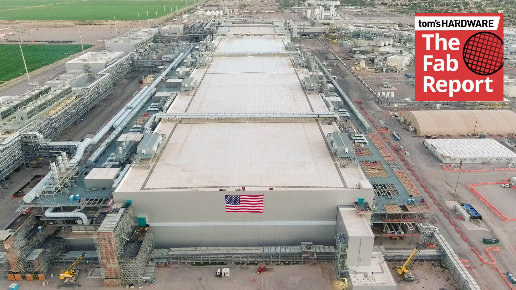
For the fourth quarter of 2026, TSMC expects revenue between $52.3 billion and $54.3 billion, which represents approximately 14% sequential growth at the midpoint. The company projects gross margin between 65% and 67%, up both sequentially and YoY.

  •  

Elon Musk calls out memory makers over 'extortionate' chip pricing, says Micron is playing smart for long-term loyalty

Elon Musk has criticized memory makers for what he calls 'extortionate' pricing amid an unprecedented shortage of both conventional DRAM and high-bandwidth memory (HBM). Although Musk did not identify the companies he criticized, his remarks seem to be directed at Samsung Electronics and SK hynix, as he praised Micron for its more 'reasonable' approach at the same time. Interestingly, Micron also enjoys exceptionally high profitability: its latest quarterly gross margin reached 81%.
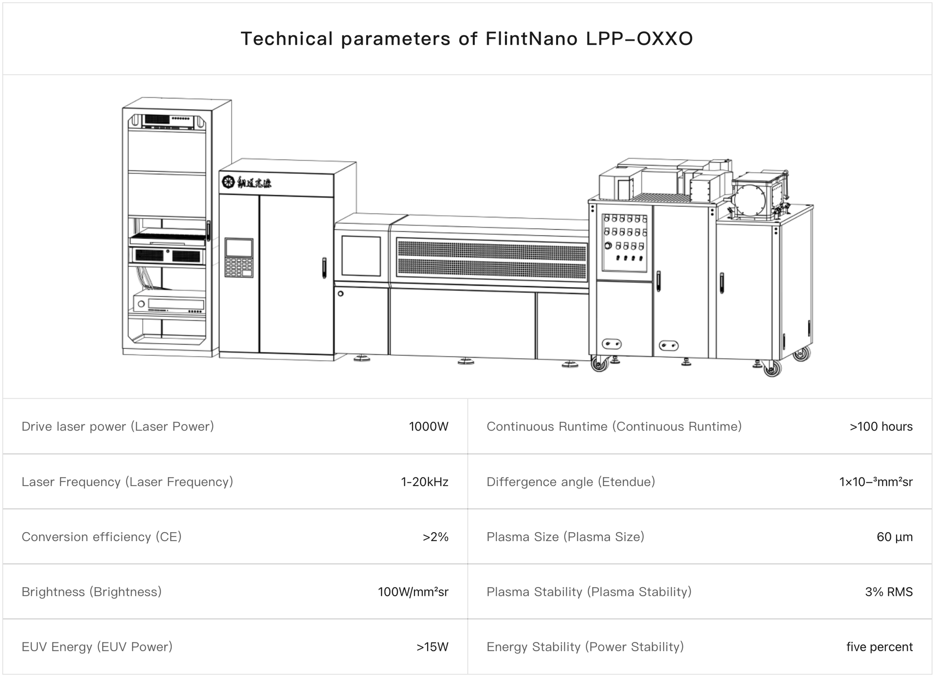
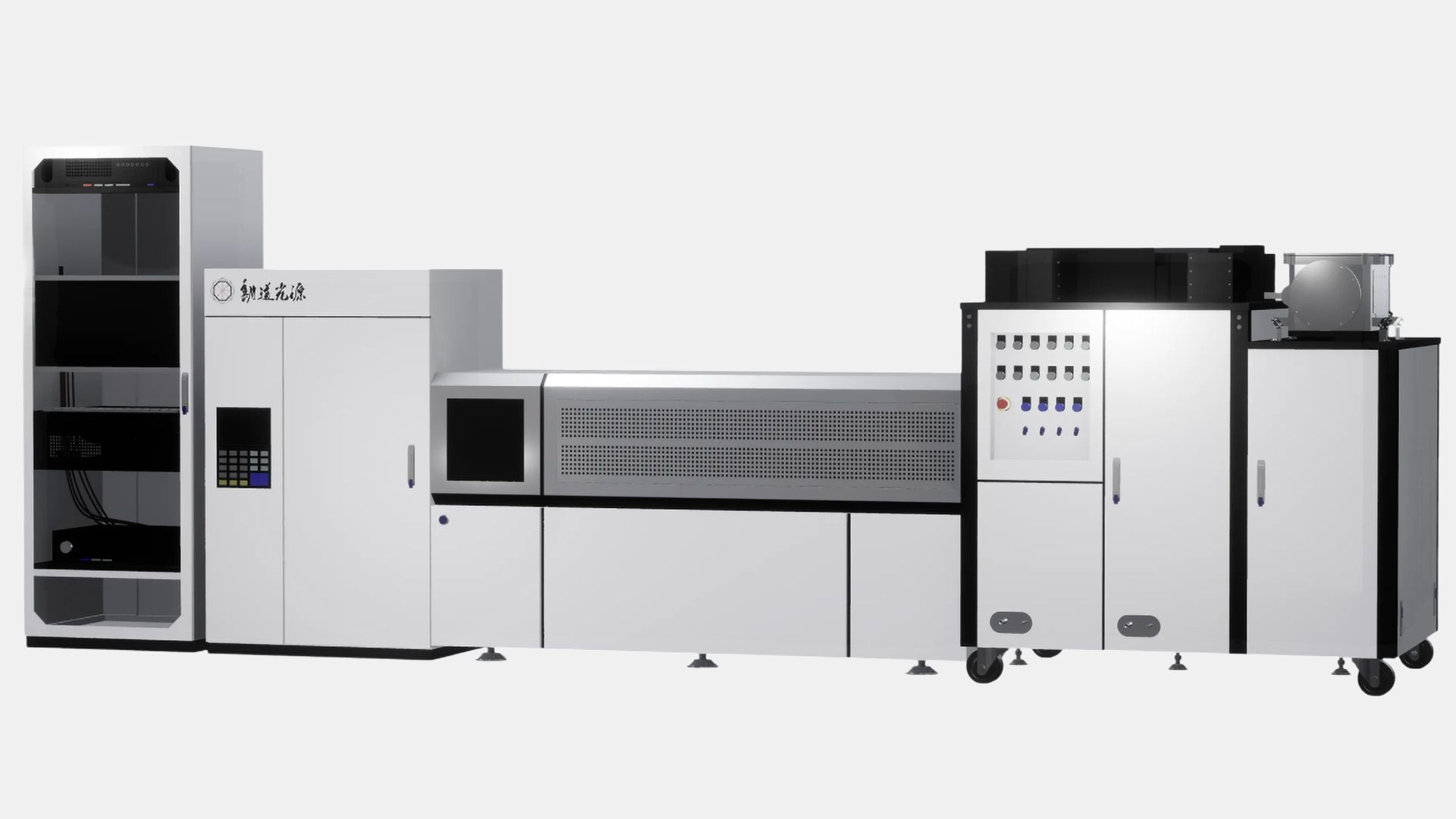
"Micron has been reasonable regarding future memory prices, while others have been extortionate, which is something today's customers will not forget," Musk wrote in a post on X. "Micron is making the smart move for long-term customer loyalty."

Musk did not provide specific details of said extortionate pricing or disclose terms offered by different memory suppliers (which tend to be confidential). Consequently, it is impossible to determine whether Samsung and SK hynix charge substantially more than does Micron for comparable products. Nevertheless, Musk's remarks suggest considerable frustration with the pricing policies of South Korean memory manufacturers.

Over the past several quarters, memory has transformed from an easy-to-obtain commodity to a strategic asset, and makers of 3D NAND and DRAM have certainly benefitted massively from this shift. Historically, memory makers have responded to strong demand and rising prices with aggressive capacity expansions, which eventually led to oversupply and falling prices. This time around, however, manufacturers have raised memory prices severalfold without comparable increases in production capacity. As a result, supply still lags behind demand and will continue to do so for years to come, which puts further upward pressure on memory prices.

What makes Musk's praise of Micron particularly interesting is the company's financial performance, which clearly suggests that the company is taking advantage of the situation in the market. In its fourth quarter of fiscal 2026, Micron reported revenue of $54.23 billion and a GAAP gross margin of 81%, up from 40% a year earlier. The company's cloud memory unit earned $16.283 billion, and its non-GAAP gross margin totaled 83%; its core data center storage business sold goods worth $18.002 billion with a 90% gross margin; while sales of the automotive and embedded units totaled $6.824 billion with gross margins reaching 84%.

Perhaps the most surprising part of Micron's last quarter report was its mobile and client revenue of $13.114 billion and non-GAAP gross margin of 90%, which means that Micron earned higher profit selling memory and storage for client devices than it did for selling memory solutions for data centers. Such results clearly indicate that even supposedly reasonable memory prices can generate extraordinary profits in the current market.

Memory manufacturers are increasingly shifting toward long-term supply agreements (LTAs) that guarantee future supply and provide customers with predictable prices of DRAM, HBM, and NAND. So far, Micron has signed 26 strategic customer agreements that cover more than 35% of its expected revenue through 2030. These contracts include $32 billion in customer financial commitments, most of which consist of cash deposits. The company acknowledges that its new agreements reflect higher prevailing memory prices, and it by no means is trying to sell memory at a discount.

Samsung has reportedly secured long-term contracts covering 75% – 80% of its planned memory output in 2027, according to South Korea's ⁠Korea Economic Daily (via @Jukan05). SK hynix is reportedly pursuing similar arrangements as AI infrastructure investments continue to absorb available memory capacity.

Market insiders and analysts expect memory supply shortages to persist through at least 2028, and that gives manufacturers considerable leverage in contract negotiations. Memory suppliers have little incentive to reduce prices and are eager to enjoy their position, but Musk's warning suggests that today’s pricing policies could influence customer relationships once supply and demand eventually return to balance.

  •